HSP45106 データシートの表示(PDF) - Intersil
部品番号
コンポーネント説明
一致するリスト
HSP45106 Datasheet PDF : 14 Pages
| |||
HSP45106
Phase Offset Adder
The output of the Phase Accumulator goes to the Phase
Offset Adder, which adds the 16-bit contents of the Phase
Offset Register to the 16 MSBs of the phase. Twenty-eight
(28) bits of the resulting 32-bit number forms the
instantaneous phase which is fed to the Sine/Cosine Section.
The user has the option of loading the Phase Offset Registers
with the contents of the Phase Input Register or with the
MOD(2:0) inputs depending on the state of PMSEL. When
PMSEL is high, the contents of the Phase Input Register are
loaded. If PMSEL is low, MOD(2:0) encode the upper 3 bits of
the Phase Offset Register while the lower 13 bits are cleared.
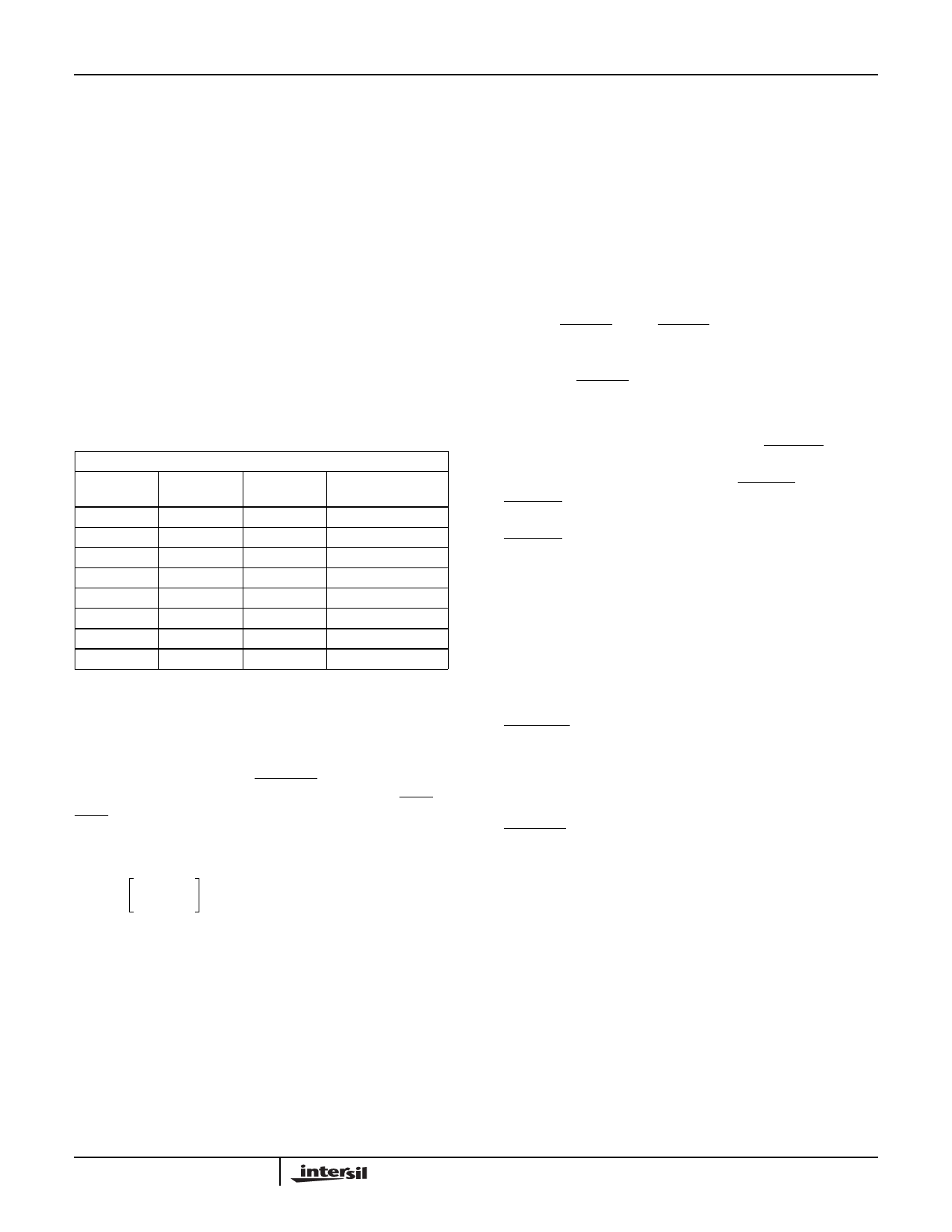
The MOD(2:0) inputs simplify PSK modulation by providing a
3 input interface to phase modulate the carrier as shown in
Table 2. The control input ENPOREG acts as a clock enable
and must be low to enable clocking of data into the Phase
Offset Register.
TABLE 2. MODULATION CONTROL MAP
MOD(2:0) DECODING
MOD2
MOD1
MOD0
PHASE SHIFT
(DEGREES)
0
0
0
0
0
0
1
45
0
1
0
90
0
1
1
135
1
0
0
270
1
0
1
315
1
1
0
180
1
1
1
225
Timer Accumulator Section
The Timer Accumulator consists of a register which is
incremented on every clock. The amount by which it
increments is loaded into the Timer Increment Input
Registers and is latched into the Timer Increment Register
on rising edges of CLK while ENTIREG is low. The output of
the Timer Accumulator is the accumulator carry out, TICO.
TICO can be used as a timer to enable the periodic sampling
of the output of the NCO-16. The number programmed into
this register equals:
N
=
INT
f-f-O-C----UL---K-T--
232
,
(EQ. 3)
where INT[x] is the integer portion of the result of the
computation.
Sine/Cosine Section
The Sine/Cosine Section (Figure 5) converts the
instantaneous phase from the PFCS Section into the
appropriate amplitude values for the sine and cosine
outputs. It takes the most significant 20 bits of the PFCS
output and passes them through a Sine/Cosine look up to
form the 16-bit quadrature outputs. The sine and cosine
values are computed to reduce the amount of ROM needed.
The magnitude of the error in the computed value of the
complex vector is less than -90.2dB. The error in the sine or
cosine alone is approximately 2dB better. The 20-bit phase
word maps into 2p radians so that the angular resolution is
(2p)/220. An address of zero corresponds to 0 radians and
an address of hex FFFFF corresponds to 2π-((2π)/220)
radians. The outputs of the Sine/Cosine Section are two's
complement sine and cosine values. The ROM contents have
been scaled by (216-1)/(216+1) for symmetry about zero.
To simplify interfacing with D/A converters, the format of the
Sine/cosine outputs may be changed to offset binary by
enabling BINFMT. When BINFMT is enabled, the MSB of the
Sine and Cosine outputs (SIN15 and COS15 when the
outputs are in parallel mode) are inverted. Depending upon
the state of BINFMT, the output is centered around midscale
and ranges from 8001H to 7FFFH (two's complement mode)
or 0001H to FFFFH (offset binary mode).
Serial output mode is chosen by enabling PAR/SER. In this
mode the user loads the Output Shift Registers with
Sine/Cosine ROM output by enabling ENPHAC. After
ENPHAC goes inactive the data is shifted out serially. For
example, to clock out one 16-bit Sine/Cosine output,
ENPHAC would be active for one cycle to load the output
Shift Register, and would then go inactive for the following 15
cycles to clock the remaining bits out. Output bit streams are
provided in formats with either MSB first or LSB first. The
MSB first format is available on the SIN15 and COS15
output pins. The LSB first format is available on the SIN0
and COS0 output pins. In MSB first format, zero’s follow the
LSB if a new output word is not loaded into the Shift
Register. In LSB first format, the sine extension bit follows
the MSB if a new data word is not loaded. The output signal
DACSTRB is provided to signal the first bit of a new output
word is valid (Figure 6). NOTE: All unused pins of
SIN(15:0) and COS(15:0) should be left floating.
A test mode is supplied which enables the user to access
the phase input to the Sine/Cosine ROM. If TEST and
PAR/SER are both high, the 28 MSBs of the phase input to
the Sine/Cosine Section are made available on SIN(15:0)
and COS(15:4). The SIN(15:0) outputs represent the MSW
of the address.
The Timing Diagrams in Figure 7, 8 and 9 show the pipeline
delays through the HSP45106 NCO16 from the time that
data is applied to the inputs until the outputs are affected by
the change. The delay is shown as a number of clock cycles,
with no attempt made to accurately represent the setup and
hold times or the clock to output delays.
8
Share Link: 