HSP45106 データシートの表示(PDF) - Intersil
部品番号
コンポーネント説明
一致するリスト
HSP45106 Datasheet PDF : 14 Pages
| |||
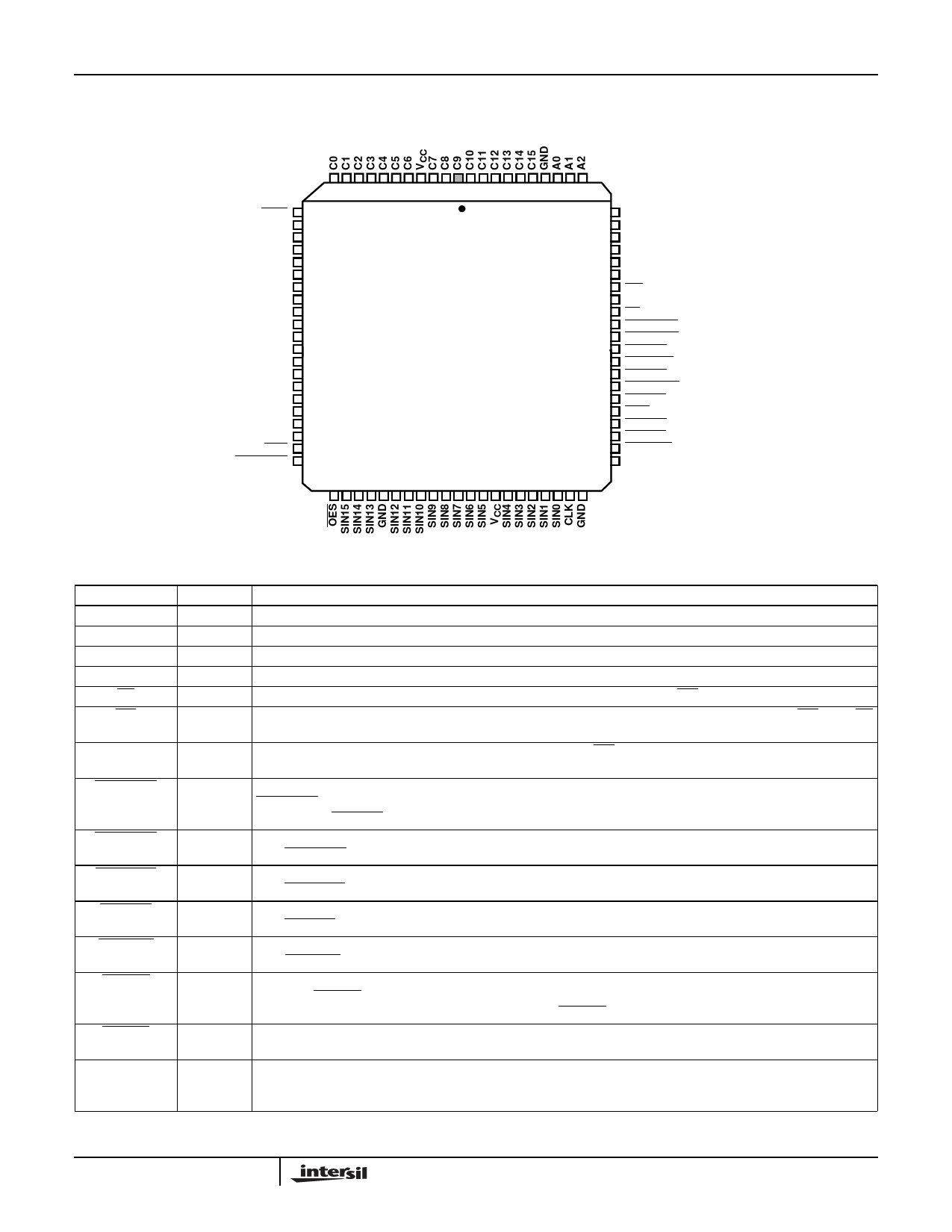
Pinouts (Continued)
HSP45106
84 LEAD PLCC
TOP VIEW
TICO
COS15
COS14
COS13
GND
COS12
COS11
COS10
COS9
COS8
COS7
COS6
COS5
COS4
VCC
COS3
COS2
COS1
COS0
OEC
DACSTRB
11 10 9 8 7 6 5 4 3 2 1 84 83 82 81 80 79 78 77 76 75
12
74
13
73
14
72
15
71
16
70
17
69
18
68
19
67
20
66
21
65
22
64
23
63
24
62
25
61
26
60
27
59
28
58
29
57
30
56
31
55
32
54
33 34 35 36 37 38 39 40 41 42 43 44 45 46 47 48 49 50 51 52 53
PMSEL
MOD0
MOD1
MOD2
TEST
VCC
WR
GND
CS
ENCFREG
ENOFREG
INHOFR
ENTIREG
INITTAC
ENPOREG
INPHAC
PACI
INITPAC
BINFMT
PAR/SER
VCC
Pin Descriptions
NAME
VCC
GND
C(15:0)
A(2:0)
CS
WR
TYPE
I
I
I
I
CLK
I
ENPOREG
I
ENOFREG
I
ENCFREG
I
ENPHAC
I
ENTIREG
I
INHOFR
I
INITPAC
I
MOD(2:0)
I
DESCRIPTION
+5 power supply pin.
Ground.
Control input bus for loading phase, frequency, and timer data into the PFCS. C0 is LSB.
Address pins for selecting destination of C(15:0) data (Table 2). A0 is the LSB
Chip select (active low). Enables data to be written into Control Registers by WR.
Write enable (active low). Data is clocked into the register selected by A(2:0) on the rising edge of WR when CS
is low.
Clock. All registers, except the Control Registers clocked with WR, are clocked (when enabled) by the rising edge
of CLK.
Phase Offset Register Enable (active low). Registered on chip by CLK. When active, after being clocked onto chip,
ENPOREG enables the clocking of data into the Phase Offset Register. Allows ROM address to be updated
regardless of ENPHAC.
Offset Frequency Register Enable (active low). Registered on chip by CLK. When active, after being clocked onto
chip, ENOFREG enables the clocking of data into the Offset Frequency Register.
Center Frequency Register Enable (active low). Registered on chip by CLK. When active, after being clocked onto
chip, ENCFREG enables the clocking of data into the Center Frequency Register.
Phase Accumulator Register Enable (active low). Registered on chip by CLK. When active, after being clocked onto
chip, ENPHAC enables the clocking of data into the Phase Accumulator Register.
Timer Increment Register Enable (active low). Registered on chip by CLK. When active, after being clocked onto
chip, ENTIREG enables the clocking of data into the Timer Increment Register.
Inhibit Offset Frequency Register Output (active low). Registered on chip by CLK. When active, after being clocked
onto chip, INHOFR zeroes the data path from the Offset Frequency Register to the Frequency Adder. New data
can be still clocked into the Offset Frequency Register. INHOFR does not affect the contents of the register.
Initialize Phase Accumulator (active low). Registered on chip by CLK. Zeroes the feedback path in the Phase
Accumulator. Does not clear the Phase Accumulator Register.
Modulation Control Inputs. When selected with the PMSEL line, these bits add an offset of 0, 45, 90, 135, 180,
225, 270, or 315 degrees to the current phase (i.e., modulate the output). The lower 13 bits of the phase control
are set to zero. These bits are registered when the Phase Offset Register is enabled.
3
Share Link: 