VSC7173XYI/G24 データシートの表示(PDF) - Maxim Integrated
部品番号
コンポーネント説明
一致するリスト
VSC7173XYI/G24
Maxim Integrated

VSC7173XYI/G24 Datasheet PDF : 17 Pages
| |||
VSC7173
Data Sheet
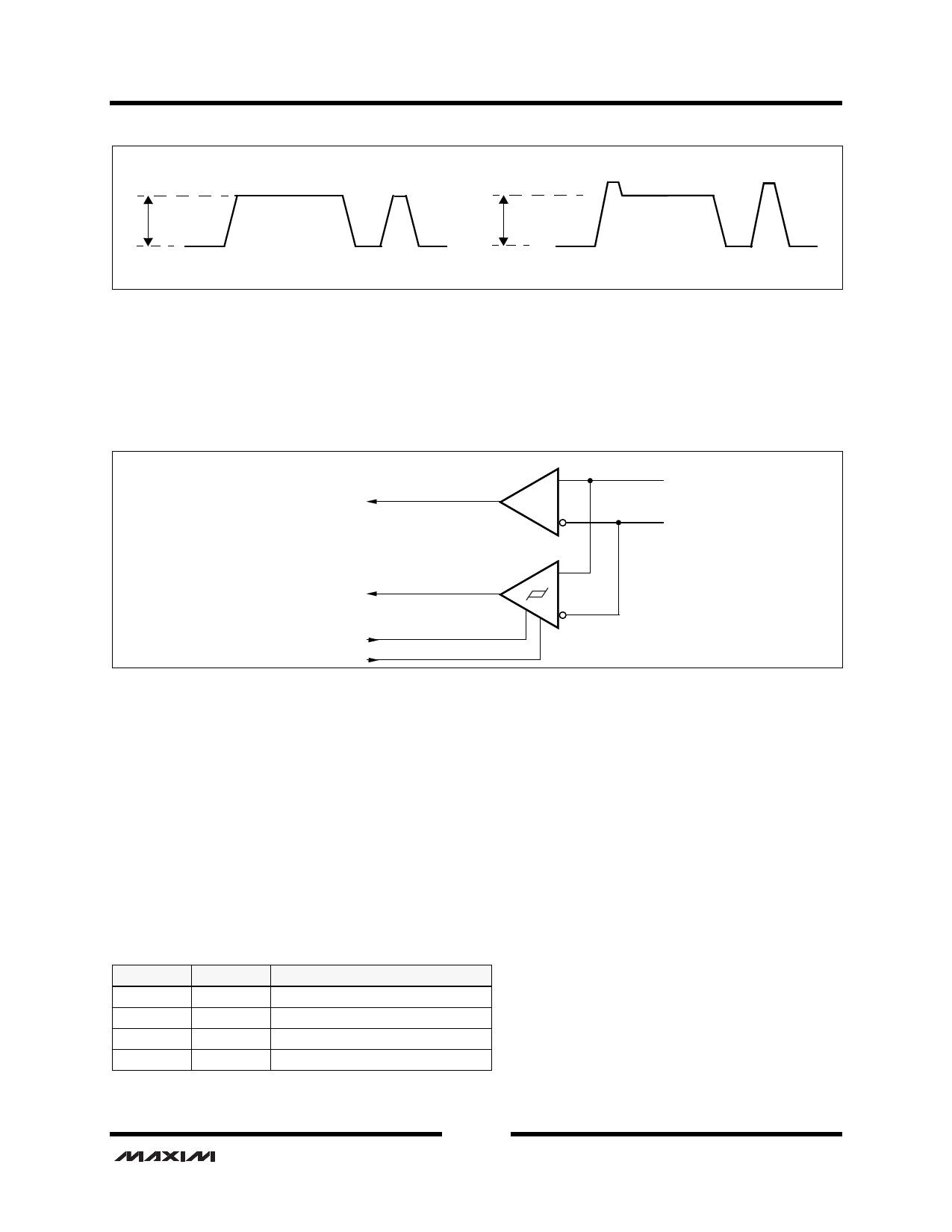
Pre-Emphasis Disabled
Pre-Emphasis Enabled
VOUT
VOUT
001 11 1 1 010
0 01 1 1 1 1 0 1 0
Figure 5. Pre-Emphasis Diagram
High-Speed Inputs
The high-speed input receivers are designed to achieve Serial ATA 1.0 compliance using AC-coupling as described in
the Serial ATA 1.0 specification. Recommended input AC-coupling capacitor values are 0.01 µF. The high-speed
input receiver contains an OOB signal detector as shown in Figure 6.
Data
Input Receiver
Input
InputN
OOB Status
(OOBPORTx signal)
OOB Detector
OOBSEL0
OOBSEL1
Figure 6. High-Speed Input Receiver
OOB Transfer
The VSC7173 cleanly transfers OOB signals from high-speed inputs to outputs. Two status outputs, OOBPORT0 and
OOBPORT1, indicate whether the input signal is data or a common-mode state. OOBPORT1 and OOBPORT1
correspond to port 0 and port 1, respectively. An OOB detector monitors the amplitude of an incoming signal in
parallel with each high-speed input. When the amplitude is less than the OOB threshold, the OOB status output is
driven HIGH. When the incoming amplitude is greater than the OOB threshold, the OOB status output is driven
LOW.
Setting the OOBSEL1 and OOBSEL0 inputs as shown in the following table configures the OOB threshold level for
all three ports.
Table 5. Setting the OOB Threshold Level
OOBSEL1
1
0
0
1
OOBSEL0
0
0
1
1
OOB THRESHOLD LEVEL
Nominal setting (150 mV to 250 mV)
Decrease by ~40 mV
Decrease by ~80 mV
Increase by ~40 mV
NOTE: All values are differential peak-to-peak voltages.
7 of 17
Confidential
Revision 4.1
May 23, 2005
Share Link: