T7264 データシートの表示(PDF) - Agere -> LSI Corporation
部品番号
コンポーネント説明
一致するリスト
T7264 Datasheet PDF : 54 Pages
| |||
T7264 U-Interface 2B1Q Transceiver
Data Sheet
April 1998
Device Interface and Connections
(continued)
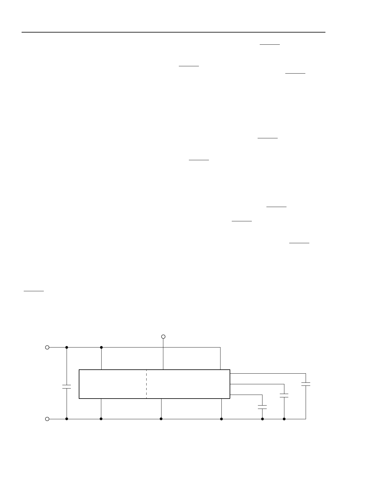
Power Supply Connections
Figure 5 shows a recommended power supply connec-
tion. C is a 10 µF capacitor. Each pair of power and
ground pins should be decoupled with 0.1 µF and
1.0 µF capacitors. Each of the three leads (VCM, VRP,
and VRN) associated with the voltage reference should
be decoupled with 0.1 µF capacitors. Place the capaci-
tors as close as possible to the power or reference and
ground pins which they decouple.
Clock Operation
The master clock for the T7264 may either be internally
generated by the on-chip crystal oscillator or supplied
by the user via the MCLK pin. In the latter case, VDDO
must be grounded. In the LT mode, an on-chip digital
phase-locked loop phase locks the F clock to the exter-
nally supplied MTC clock, unless FFC is active-low. In
NT mode, F synchronizes to the signal received from
the LT through the U-interface. If the on-chip crystal os-
cillator is used, the crystal must conform to the require-
ments given in Table 26.
Reset Operation
The T7264 can be reset via the K2 interface (issuing
afrst for three consecutive K2 frames) or via hardware
(RESET). The only difference between these two resets
is that, in the LT mode, the timing recovery filter is reset
only by a hardware reset. The RESET pin can be used
to hold the transceiver in reset indefinitely. If a hardware
reset is used when the chip is being powered up,
RESET must be held low for 1.5 ms; however, if the
chip is already powered up, then holding RESET low for
three K2 frames is sufficient.
The reset state is terminated, and the chip enters idle
mode on the K2 frame following the end of the reset sig-
nal.
Reset Sequences and Clock Synchronization
In normal use, a power-on reset can be obtained by
connecting a capacitor to the RESET pin. The internal
pull-up resistor, acting with an on-chip Schmitt trigger
on this pin, can be used to reset the chip. In this case,
the RESET waveform is shown in Figure 6.
When using this reset procedure, the various clocks
generated by the transceiver are not synchronized.
However, during testing, it can be useful to initialize all
the counters of the clock generator so that the various
clocks generated by the transceiver can be synchro-
nized to the test equipment. The RESET pin can ac-
complish this by applying the sequence shown in Figure
7. Furthermore, the RESET pin transitions should align
with falling edges of MCLK. If the internal crystal oscil-
lator is used, this can be accomplished by configuring
CKOUT for 15.36 MHz and ensuring that RESET tran-
sitions align with the falling edge of CKOUT. The user
should be aware, however, that if this clock synchroni-
zation reset sequence is used after a period of normal
operation, the phase of the clocks generated by the
T7264 (such as F, RCLKEN, C, CKOUT, etc.) may sud-
denly change as a result of the clock resynchronization.
TO VDDD (INTERNAL VCXO)
OR GNDD (EXTERNAL MCLK)
+5 V
C
SYSGND
8
VDDD
6, 17, 18
VDDO
DIGITAL
GNDD
12, 22, 27, 44
ANALOG
GNDO
19
VDDA
33, 39, 42
VCM, 28
VRP, 29
VRN, 30
GNDA
(34, 40, 41)
0.1 µF
0.1 µF
0.1 µF
5-5164a
Figure 5. Recommended Power Supply Connections
Lucent Technologies Inc.
Share Link: 