V54C3128404V データシートの表示(PDF) - Mosel Vitelic Corporation
部品番号
コンポーネント説明
一致するリスト
V54C3128404V Datasheet PDF : 45 Pages
| |||
MOSEL VITELIC
with Auto-Precharge function is initiated. The
SDRAM automatically enters the precharge opera-
tion a time delay equal to tWR (Write recovery time)
after the last data in.
Precharge Command
There is also a separate precharge command
available. When RAS and WE are low and CAS is
high at a clock timing, it triggers the precharge
operation. Three address bits, BA0, BA1 and A10
are used to define banks as shown in the following
list. The precharge command can be imposed one
clock before the last data out for CAS latency = 2,
two clocks before the last data out for CAS latency
= 3. Writes require a time delay twr from the last
data out to apply the precharge command.
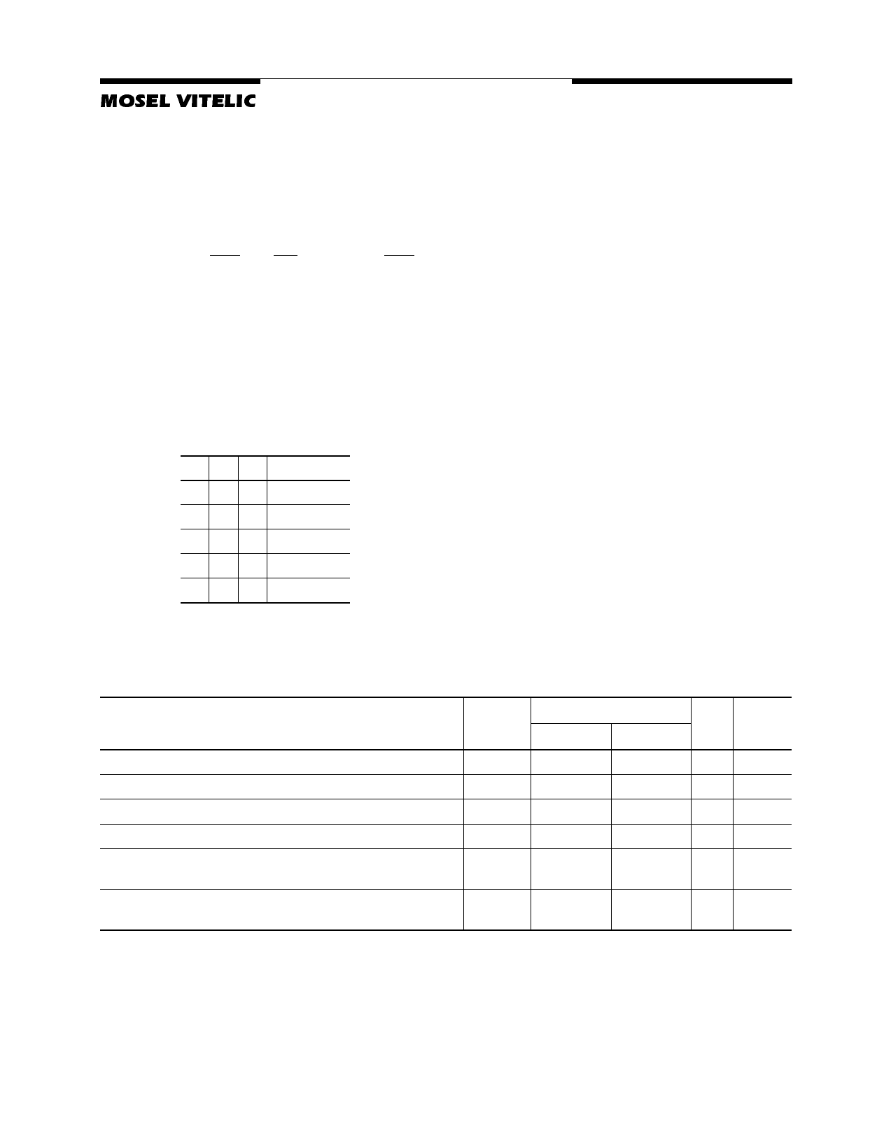
Bank Selection by Address Bits:
A10 BA0 BA1
000
001
010
011
1XX
Bank 0
Bank 1
Bank 2
Bank 3
all Banks
V54C3128(16/80/40)4V(BGA)
Burst Termination
Once a burst read or write operation has been ini-
tiated, there are several methods in which to termi-
nate the burst operation prematurely. These
methods include using another Read or Write Com-
mand to interrupt an existing burst operation, use a
Precharge Command to interrupt a burst cycle and
close the active bank, or using the Burst Stop Com-
mand to terminate the existing burst operation but
leave the bank open for future Read or Write Com-
mands to the same page of the active bank. When
interrupting a burst with another Read or Write
Command care must be taken to avoid I/O conten-
tion. The Burst Stop Command, however, has the
fewest restrictions making it the easiest method to
use when terminating a burst operation before it has
been completed. If a Burst Stop command is issued
during a burst write operation, then any residual
data from the burst write cycle will be ignored. Data
that is presented on the I/O pins before the Burst
Stop Command is registered will be written to the
memory.
Recommended Operation and Characteristics for LV-TTL
TA = 0 to 70 °C; VSS = 0 V; VCC,VCCQ = 3.3 V ± 0.3 V
Limit Values
Parameter
Symbol
min.
max. Unit Notes
Input high voltage
VIH
2.0
Vcc+0.3
V
1, 2
Input low voltage
VIL
– 0.3
0.8
V
1, 2
Output high voltage (IOUT = – 4.0 mA)
VOH
2.4
–
V
Output low voltage (IOUT = 4.0 mA)
VOL
–
0.4
V
Input leakage current, any input
(0 V < VIN < 3.6 V, all other inputs = 0 V)
II(L)
–5
5
µA
Output leakage current
(DQ is disabled, 0 V < VOUT < VCC)
IO(L)
–5
5
µA
Note:
1. All voltages are referenced to VSS.
2. VIH may overshoot to VCC + 2.0 V for pulse width of < 4ns with 3.3V. VIL may undershoot to -2.0 V for pulse width < 4.0 ns with
3.3V. Pulse width measured at 50% points with amplitude measured peak to DC reference.
V54C3128(16/80/40)4V(BGA) Rev. 1.2 September 2001
11
Share Link: 