HIP1011B データシートの表示(PDF) - Intersil
部品番号
コンポーネント説明
一致するリスト
HIP1011B Datasheet PDF : 9 Pages
| |||
HIP1011B
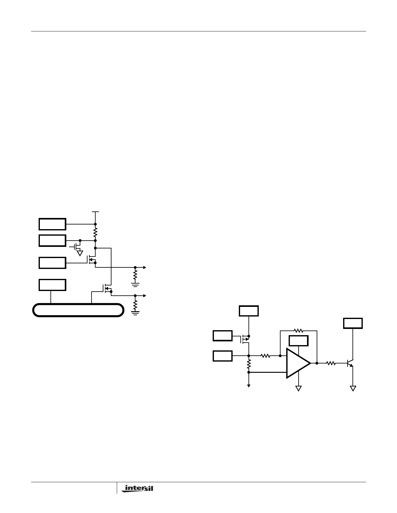
HIP1011 Split Load Application
All of the members of the HIP1011 family, including the
HIP1011B, can be used in an application where two
electrically isolated loads are to be powered from a common
bus. This may occur in a system that has a power
management feature controlled by a system controller IC
invoking a sleep or standby state. Thus one load can be shut
down while maintaining power to a second isolated circuit.
The circuit shown in Figure 7 shows the external FETs, and
sense resistor configuration for the 3.3V and/or 5V load that
has such a requirement. The HIP1011 is represented by pin
names in rectangles. Q1 and Q2 are the N-Channel FETs for
each load on this rail, these are sized appropriately for each
load. R1 and R2 are needed to pull down the supply slot pins
or load when slot power is disabled as the load discharge
FETs (Q3) on the VISEN pins are no longer attached to the
load. When power is turned off to the load these (~100Ω)
FETs turn on, thus some low current, (10mA) continues to
be drawn from the supply in addition to the sleep load
current resulting in a 4oC die temperature rise.
VSUPPLY
VS
VISEN
3V5VG
RSENSE
Q3
Q1
PWRON
Q2
SYSTEM POWER MGT CONTROLLER
TO FULL LOAD
R1
TO SLEEP LOAD
R2
FIGURE 7. SPLIT LOAD CIRCUIT
HIP1011 High Power Circuit
Instances occur when a noncompliant card is designed for
use in a PCI environment. Although the HIP1011 family has
proven to be very design flexible, controlling high power
+12V supplies requires special attention. This is due to
thermal considerations that limit the integrated power
device on the +12V supply to about 1.5A. To address this
an external add on circuit as shown in Figure 8 enables the
designer to add the OC monitoring and control of a high
power +12V supply in addition to the 3 other power
supplies. The HIP1011 is represented by pin names in
rectangles.
This circuit primarily requires that an external P-Channel
MOSFET be connected in parallel to the internal HIP1011
PMOS device and that the discrete device have a much
lower rDS(ON) value than the internal PMOS device in order
to carry the majority of the current load. By monitoring the
voltage across the sense resistor carrying the combined
load current of both the internal and external FETs and by
using a comparator with a common mode input voltage
range to the positive rail and a low input voltage threshold
offset to reduce distribution losses, a high precision OC
detector can be designed to control a much higher current
load than can be tolerated by the HIP1011.
An alternative circuit for moderate current levels where both
accuracy and cost are lowered can be accomplished by a
single external P-Channel MOSFET in parallel with the
internal P-Channel MOSFET. For example, if 2X the OC level
is desired a 0.3Ω rDS(ON) P-Channel MOSFET can be used
thus approximately doubling the +12 IOUT before latch-off.
IOCTOTAL = IOCINTERNAL (1 + rDS(ON) of internal
FET/rDS(ON) of external FET).
12VIN
12VG
Q1
12VO
R1
RSENSE
R2
12VIN
+
-
FLTN
R3
Q2
TO +12V LOAD
FIGURE 8. HIGH POWER +12V CIRCUIT
8
FN4640.5
November 18, 2004
Share Link: 