HIP1011B データシートの表示(PDF) - Intersil
部品番号
コンポーネント説明
一致するリスト
HIP1011B Datasheet PDF : 9 Pages
| |||
HIP1011B
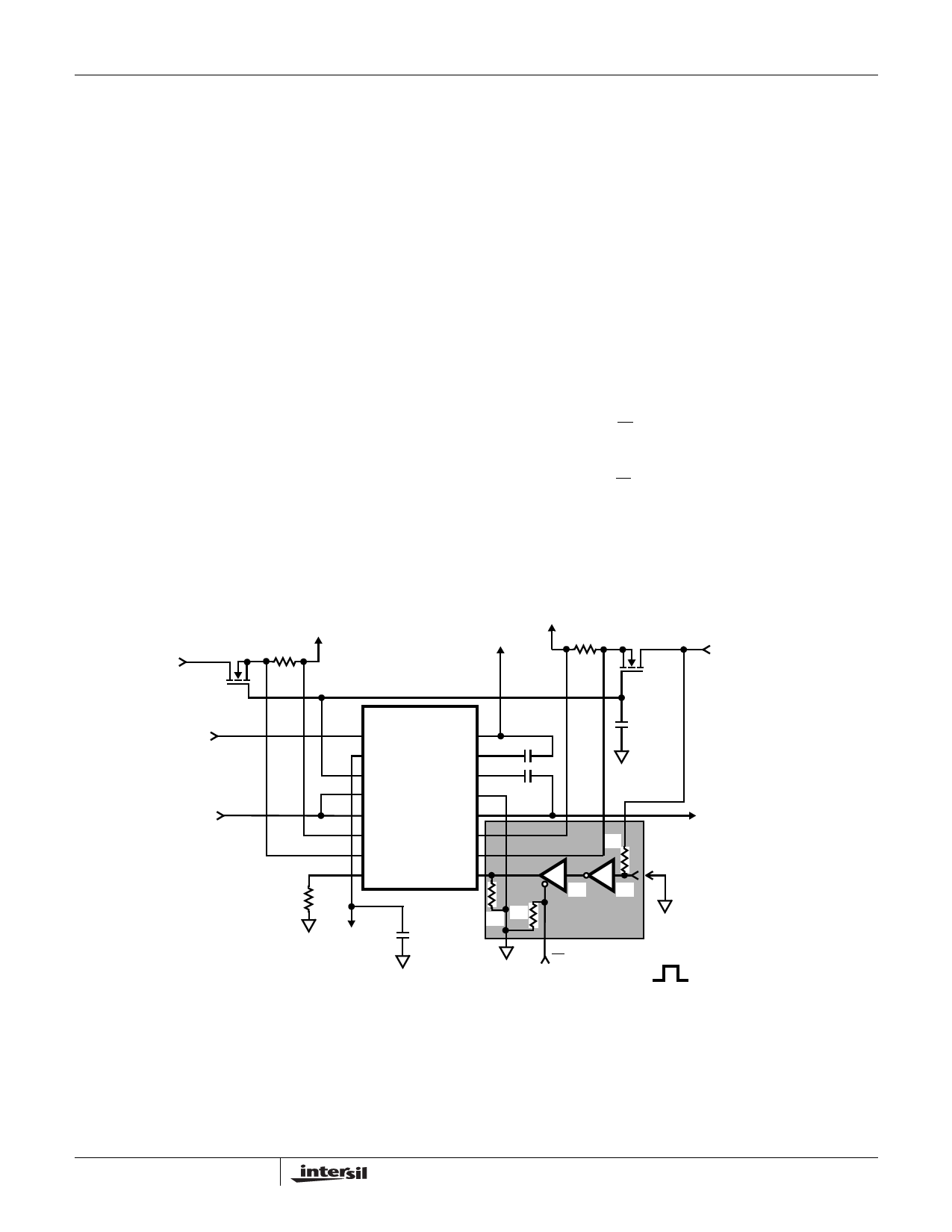
Applications
Implementing the HIP1011B in the CompactPCI
Hot Swap Application
This application offers to the CompactPCI peripheral board
designer programmable Over Current (OC) protection,
programmable delays to latch off, and soft start ramp turn on
for all four supplies with simultaneous latch off upon OC fault
detection.
Figure 6 illustrates the HIP1011EVAL2 evaluation board for
CompactPCI Hot Swap implementation. The shaded
components are the external components necessary to
accomplish both controlled power up and turn-on. For
minimum PCB area single gate logic can be used.
Insertion Sequence
Because of the staggered pin lengths in the CompactPCI
connector, as the board is inserted into the slot, the ground
bus plane is connected first via the longest pins referencing
the HIP1011B by way of the PWRON, OCSET and GND pins
through R4 and R3. Additionally the three-state driver, U1
address line is referenced through R6.
Subsequently the medium length pins engage to connect the
+3.3V, +5V, +12V, -12V lines to the inputs, activating the
HIP1011B, and the 2 logic devices, U1 and U2. At this time the
HIP1011B is in control holding off all the MOSFET switches, as
3.3V INPUT
3.3VOUT
R2
PWRON is being held low. With the logic devices powered the
inverter U2 input is pulled high putting a low on the three-state
driver U1 input which is passed through to the PWRON pin.
Upon complete insertion the shortest length pin, “board
present” which is tied to ground on the backplane finally
contacts the inverter input. The inverter output pulls high
turning on the HIP1011B through U1 thus, the board is fully
powered on only upon complete insertion.
Fault Reset
If an overcurrent condition is detected on the board by the
HIP1011B the FLTN signal transitions low, once the
VFLTN,TH is reached all the switches are simultaneously
switched off protecting the system, the board and its
components. The system controller is notified of the fault
occurrence by the FLTN signal.
Reset of the faulted card is accomplished by a positive pulse
on the three-state oe input. The pulse puts U1 output into a
high Z state allowing R4 to pull the HIP1011B PWRON pin
low, resetting the HIP1011B. The HIP1011B switches turn
back on when U1 oe input returns to a low state resulting in
PWRON going high. The reset pulse can be generated by
either the system restart/reset to the master board or from
the master system board to any of the peripheral boards in
the system.
-12VOUT 5VOUT
R1
5V INPUT
Q1, Q2
-12V INPUT
12V INPUT
Q3, Q4
HIP1011
M12VIN M12VO
FLTN
M12VG
3V5VG
12VG
VCC
GND
12VIN
12VO
3VISEN 5VISEN
3VS
5VS
R3
OCSET PWRON
C3
C1
C2
R5
U1
U2
FLTN
C4
R4 R6
oe
PULSE HIGH TO RESET FAULT
+12VOUT
BOARD PRESENT
PIN ON
BACKPLANE
NOTES:
FIGURE 6. HIP1011B CompactPCI APPLICATION CIRCUIT
3. Each test point (TP) on HIP1011EVAL2 refers to device pin number.
4. SIGNAL_GND, SHIELD_GND and SHORTPIN_GND can be jumpered together for ease of evaluation.
5. HIP1011B devices can be placed into HIP1011EVAL2 board for evaluation or contact INTERSIL for a HIP1011B equipped evaluation board.
7
FN4640.5
November 18, 2004
Share Link: 