P4C164-10JI データシートの表示(PDF) - Performance Semiconductor
部品番号
コンポーネント説明
一致するリスト
P4C164-10JI Datasheet PDF : 8 Pages
| |||
P4C164/164L
AC ELECTRICAL CHARACTERISTICS—READ CYCLE
(VCC = 5V ± 10%, All Temperature Ranges)(2)
Sym.
Parameter
-8
-10
-12
-15
-20
-25
-35
-45 Unit
Min Max Min Max Min Max Min Max Min Max Min Max Min Max Min Max
tRC Read Cycle Time 8
10
12
15
20
25
35
45
ns
tAA Address Access
8
10
12
15
20
25
35
45 ns
Time
tAC Chip Enable
Access Time
8
10
12
15
20
25
35
45 ns
tOH Output Hold from 3
3
3
3
3
3
3
3
ns
Address Change
t
LZ
Chip Enable to
2
2
2
2
2
2
2
2
ns
Output in Low Z
tHZ Chip Disable to
5
6
7
8
8
10
15
20 ns
Output in High Z
tOE Output Enable
Low to Data
Valid
5
6
7
9
10
13
18
20 ns
tOLZ Output Enable
2
2
2
2
2
2
2
2
ns
Low to Low Z
tOHZ Output Enable
High to High Z
5
6
7
9
9
12
15
20 ns
tPU Chip Enable to 0
0
0
0
0
0
0
0
ns
Power Up Time
tPD Chip Disable to
Power Down
Time
8
10
12
15
20
20
20
25 ns
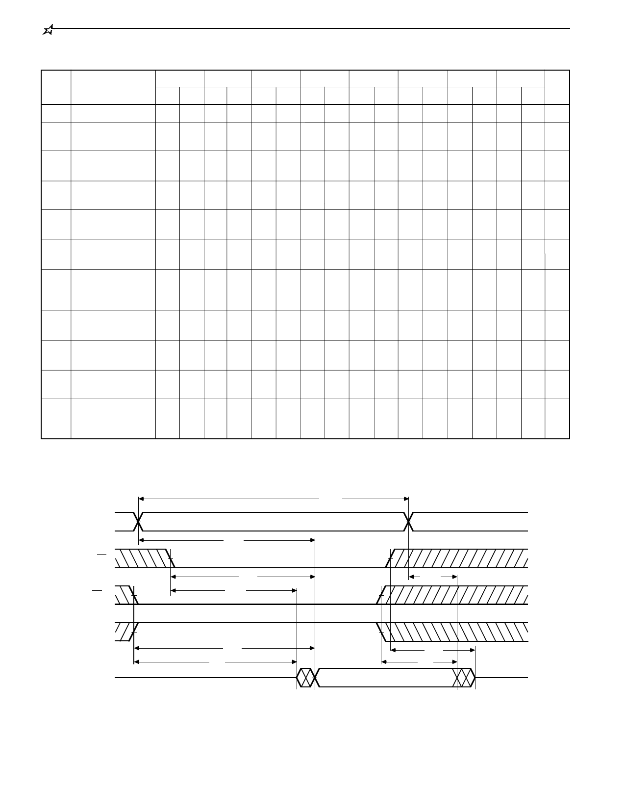
READ CYCLE NO. 1 (OE CONTROLLED)(5)
(9)
t RC
ADDRESS
t AA
OE
t OE
t OH
CE1
tOLZ (8)
CE2
DATA OUT
t AC
tLZ (8)
t
(8)
OHZ
t
(8)
HZ
Notes:
5. WE is HIGH for READ cycle.
6.
CE
1
is
LOW,
CE2
is
HIGH
and
OE
is
LOW
for
READ
cycle.
7.
ADDRESS
must
be
valid
prior
to,
or
coincident
with
CE
1
transition
LOW and CE2 transition HIGH.
8. Transition is measured ± 200 mV from steady state voltage prior to
change, with loading as specified in Figure 1. This parameter is
sampled and not 100% tested.
94
Share Link: 