P4C164-10JI データシートの表示(PDF) - Performance Semiconductor
部品番号
コンポーネント説明
一致するリスト
P4C164-10JI Datasheet PDF : 8 Pages
| |||
P4C164/P4C164L
ULTRA HIGH SPEED 8K x 8
STATIC CMOS RAMS
P4C164/164L
FEATURES
Full CMOS, 6T Cell
High Speed (Equal Access and Cycle Times)
– 8/10/12/15/20/25 ns (Commercial)
– 10/12/15/20/25/35 (Industrial)
– 12/15/20/25/35/45 ns (Military)
Low Power Operation
– 770mW Active –15
– 660/743 mW Active – 20
– 495/575 mW Active – 25, 35, 45
– 193/220 mW Standby (TTL Input)
– 5.5mW Standby (CMOS Input) P4C164L (Military)
Output Enable and Dual Chip Enable Control
Functions
Single 5V±10% Power Supply
Data Retention with 2.0V Supply, 10 µA Typical
Current (P4C164L Military)
Common Data I/O
Fully TTL Compatible Inputs and Outputs
Standard Pinout (JEDEC Approved)
– 28-Pin 300 mil DIP, SOJ
– 28-Pin 600 mil Ceramic DIP
– 28-Pin 350 x 550 mil LCC
– 28-Pin CERPACK
DESCRIPTION
The P4C164 and P4C164L are 65,536-bit ultra high-speed
static RAMs organized as 8K x 8. The CMOS memories
require no clocks or refreshing and have equal access and
cycle times. Inputs are fully TTL-compatible. The RAMs
operate from a single 5V±10% tolerance power supply.
With battery backup, data integrity is maintained with
supply voltages down to 2.0V. Current drain is typically 10
µA from a 2.0V supply.
Access times as fast as 10 nanoseconds are available,
permitting greatly enhanced system operating speeds. In
full standby mode with CMOS inputs, power consumption
is only 5.5 mW for the P4C164L.
The P4C164 and P4C164L are available in 28-pin 300 mil
DIP and SOJ, 28-pin 600 mil ceramic DIP, and 28-pin 350
x 550 mil LCC packages providing excellent board level
densities.
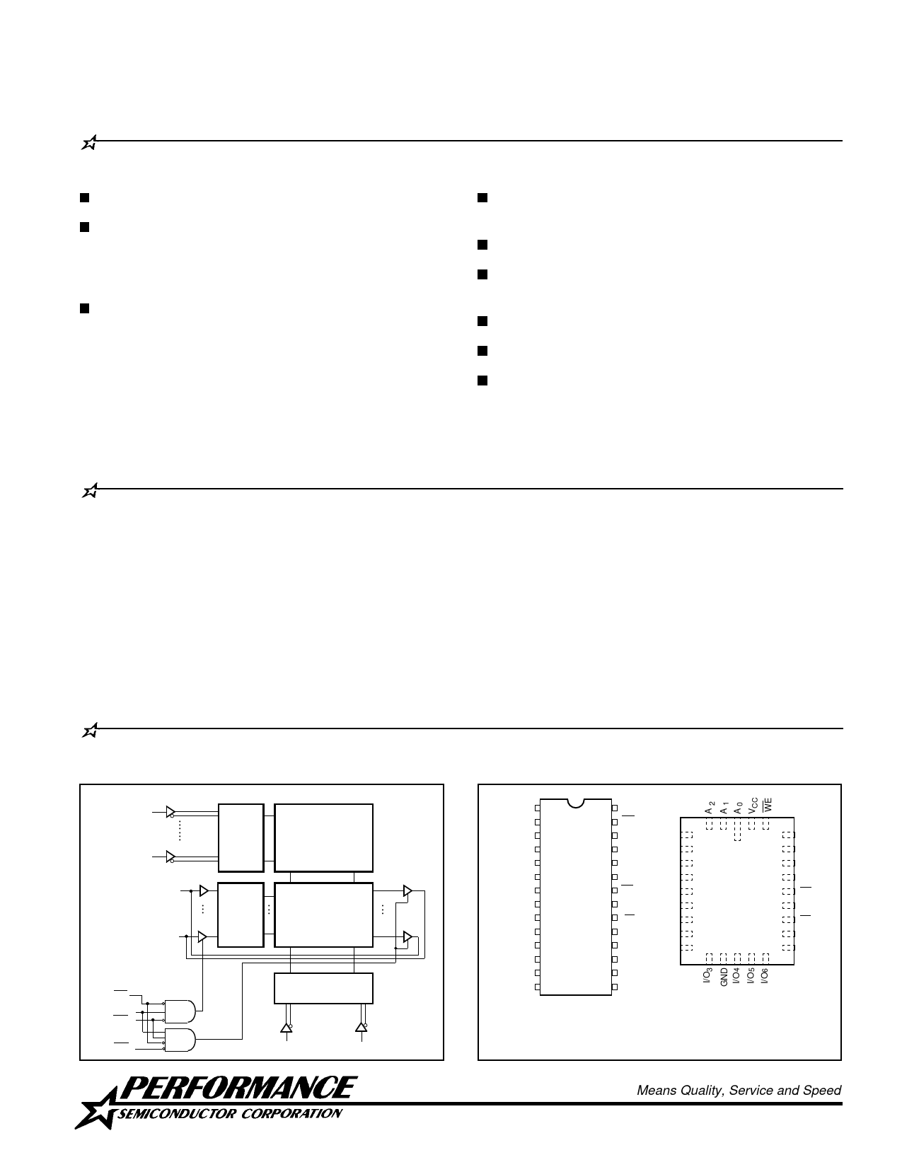
FUNCTIONAL BLOCK DIAGRAM
A0
A7
I/O 1
I/O 8
ROW
SELECT
65,536-BIT
MEMORY
ARRAY
INPUT
DATA
CONTROL
COLUMN I/O
CE 1
CE 2
WE
OE
COLUMN
SELECT
••••••
A8
A12
PIN CONFIGURATIONS
NC 1
A0 2
A1 3
A2 4
A3 5
A4 6
A5 7
A6 8
A7 9
A 8 10
I/O1 11
I/O2 12
I/O3 13
GND 14
28 VCC
27 WE
26 CE 2
25 A12
24 A 11
23 A10
22 OE
21 A 9
20 CE1
19 I/O 8
18 I/O 7
17 I/O 6
16 I/O 5
15 I/O 4
NC
A3
A4
A5
A6
A7
A8
I/O 1
I/O 2
1519B
3
27
4 2 28 26 CE2
5
1
25
A 12
6
24
A 11
7
23
A 10
8
22 OE
9
21 A 9
10
20 CE1
11
19 I/O8
12 14 15 16 18
I/O7
13
17
1519C
DIP (P5, D5-2, D5-1), SOJ (J5) 1519B
LCC (L5)
CERPACK (F4) SIMILAR
TOP VIEW
1519A
TOP VIEW
Means Quality, Service and Speed
1Q97
91
Share Link: 