P4C1981-25JC データシートの表示(PDF) - Semiconductor Corporation
部品番号
コンポーネント説明
一致するリスト
P4C1981-25JC Datasheet PDF : 13 Pages
| |||
P4C1981/1981L, P4C1982/1982L
POWER DISSIPATION CHARACTERISTICS VS. SPEED
Symbol
Parameter
ICC Dynamic Operating Current*
Temperature
Range
Commercial
Industrial
Military
–10 –12 –15 –20 –25 –35 –45 Unit
180 170 160 155 150 N/A N/A mA
N/A 180 170 160 155 150 N/A mA
N/A N/A 170 160 155 150 145 mA
*VCC = 5.5V. Tested with outputs open. f = Max. Switching inputs are 0V and 3V.
CE1 = VIL, CE2 = VIL, OE = VIH
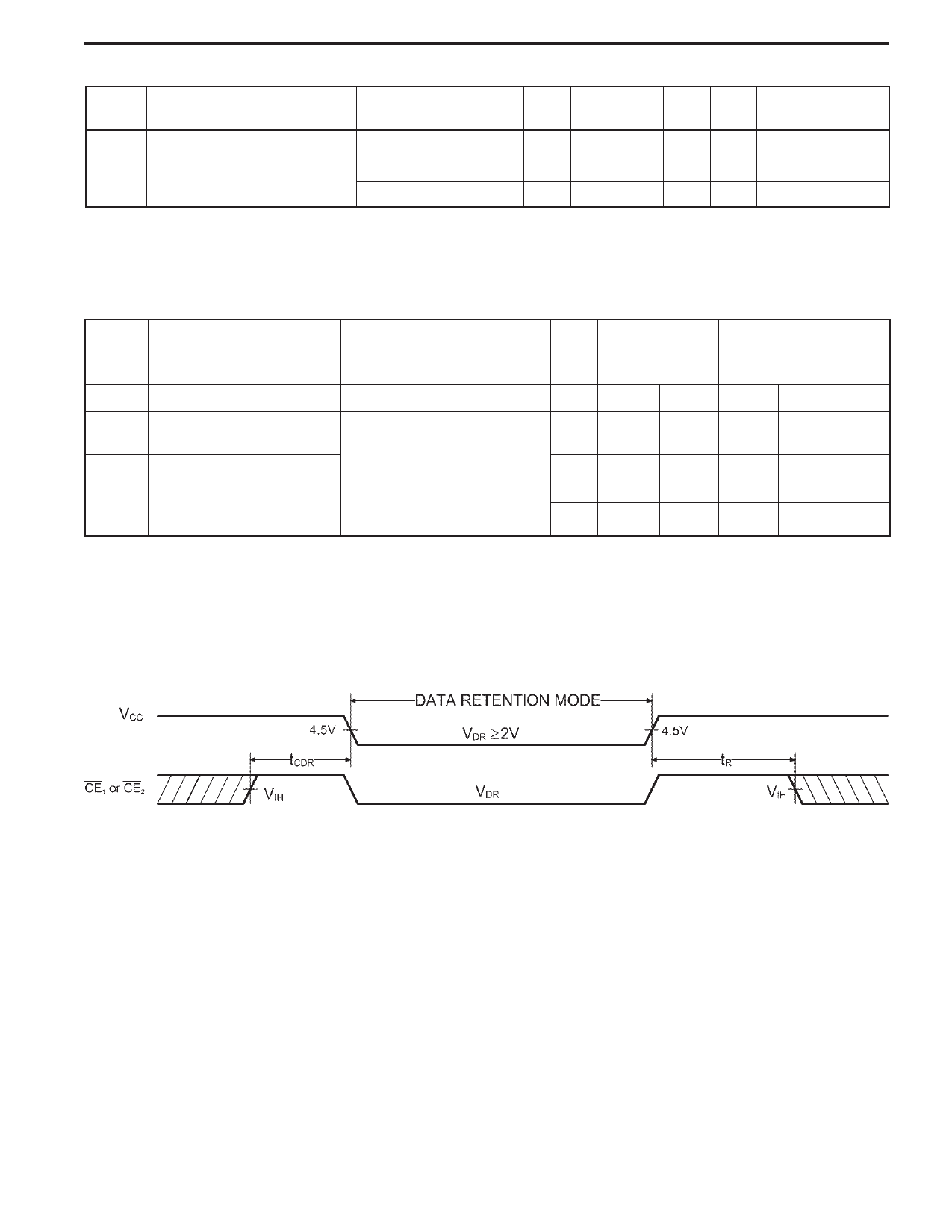
DATA RETENTION CHARACTERISTICS (P4C1981L/P4C1982L Military Temperature Only)
Symbol
Parameter
VDR
ICCDR
VCC for Data Retention
Data Retention Current
Test Condition
Typ.*
Max
Min
VCC=
VCC=
Unit
2.0V 3.0V 2.0V 3.0V
2.0
V
10
15 600 900 µA
tCDR
Chip Deselect to
CE1 or CE2 ≥ VCC – 0.2V,
0
ns
Data Retention Time
VIN ≥ VCC – 0.2V or
tR†
Operation Recovery Time VIN ≤ 0.2V
tRC§
ns
*TA = +25°C
§tRC = Read Cycle Time
†This parameter is guaranteed but not tested.
DATA RETENTION WAVEFORM
Notes:
1. Stresses greater than those listed under MAXIMUM RATINGS may
cause permanent damage to the device. This is a stress rating only
and functional operation of the device at these or any other conditions
above those indicated in the operational sections of this specification
is not implied. Exposure to MAXIMUM ratingconditions for extended
periods may affect reliability.
2. Extended temperature operation guaranteed with 400 linear feet per
minute of air flow.
3. Transient inputs with VIL and IIL not more negative than –3.0V and
–100mA, respectively, are permissible for pulse widths up to 20 ns.
4. This parameter is sampled and not 100% tested.
Document # SRAM114 REV B
Page 3 of 13
Share Link: 