HS45116GM-25 データシートの表示(PDF) - Intersil
部品番号
コンポーネント説明
一致するリスト
HS45116GM-25 Datasheet PDF : 6 Pages
| |||
HSP45116/883
Absolute Maximum Ratings
Supply Voltage. . . . . . . . . . . . . . . . . . . . . . . . . . . . . . . . . . . . . +8.0V
Input or Output Voltage Applied. . . . . . . . . GND -0.5V to VCC +0.5V
ESD Rating Classification . . . . . . . . . . . . . . . . . . . . . . . . . . . Class 1
Operating Conditions
Temperature Range. . . . . . . . . . . . . . . . . . . . . . . . . -55oC to 125oC
Supply Range . . . . . . . . . . . . . . . . . . . . . . . . . . . . . +4.5V to +5.5V
Thermal Information
Thermal Resistance (Typical, Note 1)
θJA (oC/W) θJC (oC/W)
PGA Package . . . . . . . . . . . . . . . . . . .
30.0
5.0
Maximum Package Power Dissipation at 125oC
PGA Package . . . . . . . . . . . . . . . . . . . . . . . . . . . . . . . . . . . 2.16W
Maximum Junction Temperature . . . . . . . . . . . . . . . . . . . . . . . 175oC
Maximum Storage Temperature Range . . . . . . . . . . -65oC to 150oC
Maximum Lead Temperature (Soldering 10s) . . . . . . . . . . . . 300oC
Number of Transistors or Gates . . . . . . . . . . . . 103,000 Transistors
CAUTION: Stresses above those listed in “Absolute Maximum Ratings” may cause permanent damage to the device. This is a stress only rating and operation of the
device at these or any other conditions above those indicated in the operational sections of this specification is not implied.
NOTE:
1. θJA is measured with the component mounted on an evaluation PC board in free air.
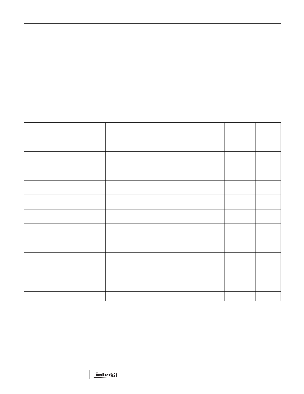
TABLE 1. DC ELECTRICAL PERFORMANCE SPECIFICATIONS
Device Guaranteed and 100% Tested
PARAMETER
SYMBOL
TEST
CONDITIONS
GROUP A
SUBGROUPS TEMPERATURE (oC) MIN
MAX
UNITS
Logical One Input
Voltage
VIH
VCC = 5.5V
1, 2, 3
55 ≤ TA ≤ 125
2.2
-
V
Logical Zero Input
Voltage
VIL
VCC = 4.5V
1, 2, 3
55 ≤ TA ≤ 125
-
0.8
V
Logical One Input
Voltage Clock
VIHC
VCC = 5.5V
1, 2, 3
55 ≤ TA ≤ 125
3.0
-
V
Logical Zero Input
Voltage Clock
VILC
VCC = 4.5V
1, 2, 3
55 ≤ TA ≤ 125
-
0.8
V
Output HIGH Voltage
Output LOW Voltage
Input Leakage Current
VOH
VOL
II
IOH = -400µA
VCC = 4.5V (Note 2)
IOL = +2.0mA
VCC = 4.5V (Note 2)
VIN = VCC or GND VCC
= 5.5V
1, 2, 3
1, 2, 3
1, 2, 3
55 ≤ TA ≤ 125
2.6
-
V
55 ≤ TA ≤ 125
-
0.4
V
55 ≤ TA ≤ 125
-10 +10
µA
Output or I/O Leakage
Current
Standby Power Supply
Current
IO
ICCSB
VOUT = VCC or GND
VCC = 5.5V
VIN = VCC or GND, VCC
= 5.5V, (Note 5)
1, 2, 3
1, 2, 3
55 ≤ TA ≤ 125
-10 +10
µA
55 ≤ TA ≤ 125
-
500
µA
Operating Power Supply
Current
ICCOP
f = 15MHz,
VIN = VCC or GND
VCC = 5.5V
(Notes 3, 5)
1, 2, 3
55 ≤ TA ≤ 125
-
150
mA
Functional Test
FT
(Note 4)
7, 8
55 ≤ TA ≤ 125
-
-
NOTES:
2. Interchanging of force and sense conditions is permitted.
3. Operating Supply Current is proportional to frequency, typical rating is 10mA/MHz.
4. Tested as follows: f = 1MHz, VIH (clock inputs) = 3.4V, VIH (all other inputs) = 2.6V, VIL = 0.4V, VOH ≥ 1.5V, and VOL ≤ 1.5V.
5. Output per test load circuit with switch open and CL = 40pF.
2
Share Link: 