IMIC9530CT データシートの表示(PDF) - Silicon Laboratories
部品番号
コンポーネント説明
一致するリスト
IMIC9530CT Datasheet PDF : 10 Pages
| |||
C9530
Serial Data Interface
To enhance the flexibility and function of the clock synthesizer,
a two-signal serial interface is provided. Through the Serial
Data Interface, various device functions, such as individual
clock output buffers, can be individually enabled or disabled.
The registers associated with the Serial Data Interface
initialize to their default setting upon power-up, and therefore
use of this interface is optional. Clock device register changes
are normally made upon system initialization, if any are
required.
Data Protocol
The clock driver serial protocol accepts block write a opera-
tions from the controller. The bytes must be accessed in
sequential order from lowest to highest byte (most significant
bit first) with the ability to stop after any complete byte has
been transferred. The C9530 does not support the Block Read
function.
The block write protocol is outlined in Table 2. The addresses
are listed in Table 3.
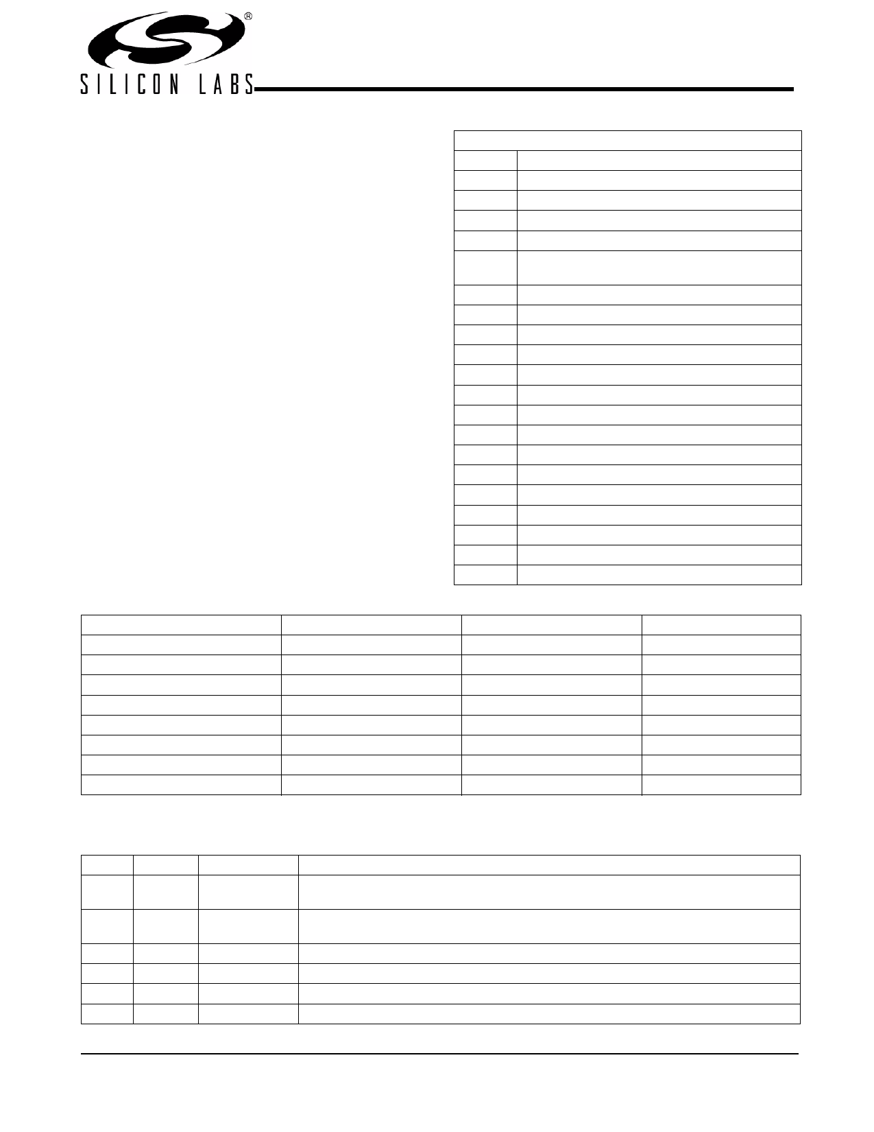
Table 2. Block Read and Block Write Protocol
Block Write Protocol
Bit
Description
1 Start
2:8 Slave address – 7 bits
9 Write = 0
10
11:18
19
20:27
28
29:36
37
Acknowledge from slave
Command Code – 8 bits
‘00000000’ stands for block operation
Acknowledge from slave
Byte Count – 8 bits
Acknowledge from slave
Data byte 1 – 8 bits
Acknowledge from slave
38:45
46
....
....
....
....
....
....
Data byte 2 – 8 bits
Acknowledge from slave
......................
Data Byte (N–1) – 8 bits
Acknowledge from slave
Data Byte N – 8 bits
Acknowledge from slave
Stop
Table 3. SMBus Address Selection Table
SMBus Address of the Device
DE
IA0 Bit (Pin 10)
0
DC
1
DA
0
D8
1
D6
0
D4
1
D0
0
D2
1
IA1 Bit (Pin 11)
0
0
1
1
0
0
1
1
IA2 Bit (Pin 12)
0
0
0
0
1
1
1
1
Serial Control Registers
Byte 0: Function Select Register
Bit @Pup
7
1
Name
TESTEN
6
0
SSEN
5
1
4
0
3
0
2
0
SSSEL
S1
S0
Description
Test Mode Enable.
1 = Normal operation, 0 = Test mode
Spread Spectrum modulation control bit (effective only when Bit 0 of this register is set to
a 0) 0 = OFF, 1= ON
SSCG Spread width select. 1 = 0.5%, 0 = 1.0% See Table 4 below for clarification
SB1 Bank MSB frequency control bit (effective only when Bit 0 of this register is set to a 0)
SB0 Bank LSB frequency control bit (effective only when Bit 0 of this register is set to a 0)
SA1 Bank MSB frequency control bit (effective only when Bit 0 of this register is set to a 0)
.......................Document #: 38-07033 Rev. *C Page 3 of 10
Share Link: 