AAT3190 データシートの表示(PDF) - Advanced Analogic Technologies
部品番号
コンポーネント説明
一致するリスト
AAT3190 Datasheet PDF : 16 Pages
| |||
AAT3190
Positive/Negative Charge Pump for Voltage Bias
IN
OSC
CTL
C7 1/2 A4
DRVN
BAT54SDW
FBN
AAT3190
GND
VREF
1.2V
R1
R2
C2
VON = -(R1/R2) x VREF
VON
C10
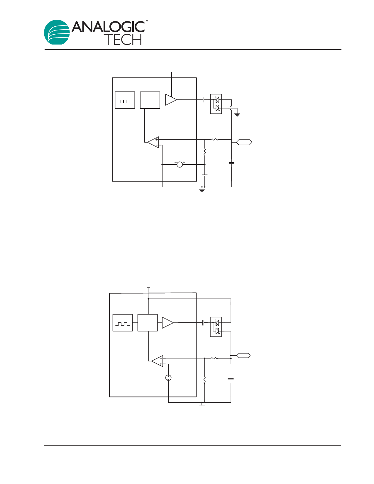
Figure 1: Negative Charge Pump Block Diagram.
Positive Charge Pump
During the first half-cycle, the N-channel MOSFET
turns on and charges the flying capacitor C4
(Figure 2). During the second half-cycle, the N-
channel MOSFET turns off and the P-channel
MOSFET turns on, level shifting C4 by the input
voltage. This connects C4 in parallel with the reser-
voir capacitor C5. If the voltage across C5 plus a
diode drop is less than the level shifted flying
capacitor (C4 + VIN), charge is transferred from C4
to C5 until the diode turns off.
IN
OSC
CTL
AAT3190
VREF
1.2V
GND
VIN
C4 1/2 A3
DRVP
BAT54SDW
FBP
R3
VOP
VOP = (1+R3/R4) x VREF
R4
C5
Figure 2: Positive Charge Pump Block Diagram.
3190.2006.01.1.2
9
Share Link: 