AAT3190 データシートの表示(PDF) - Advanced Analogic Technologies
部品番号
コンポーネント説明
一致するリスト
AAT3190 Datasheet PDF : 16 Pages
| |||
AAT3190
Positive/Negative Charge Pump for Voltage Bias
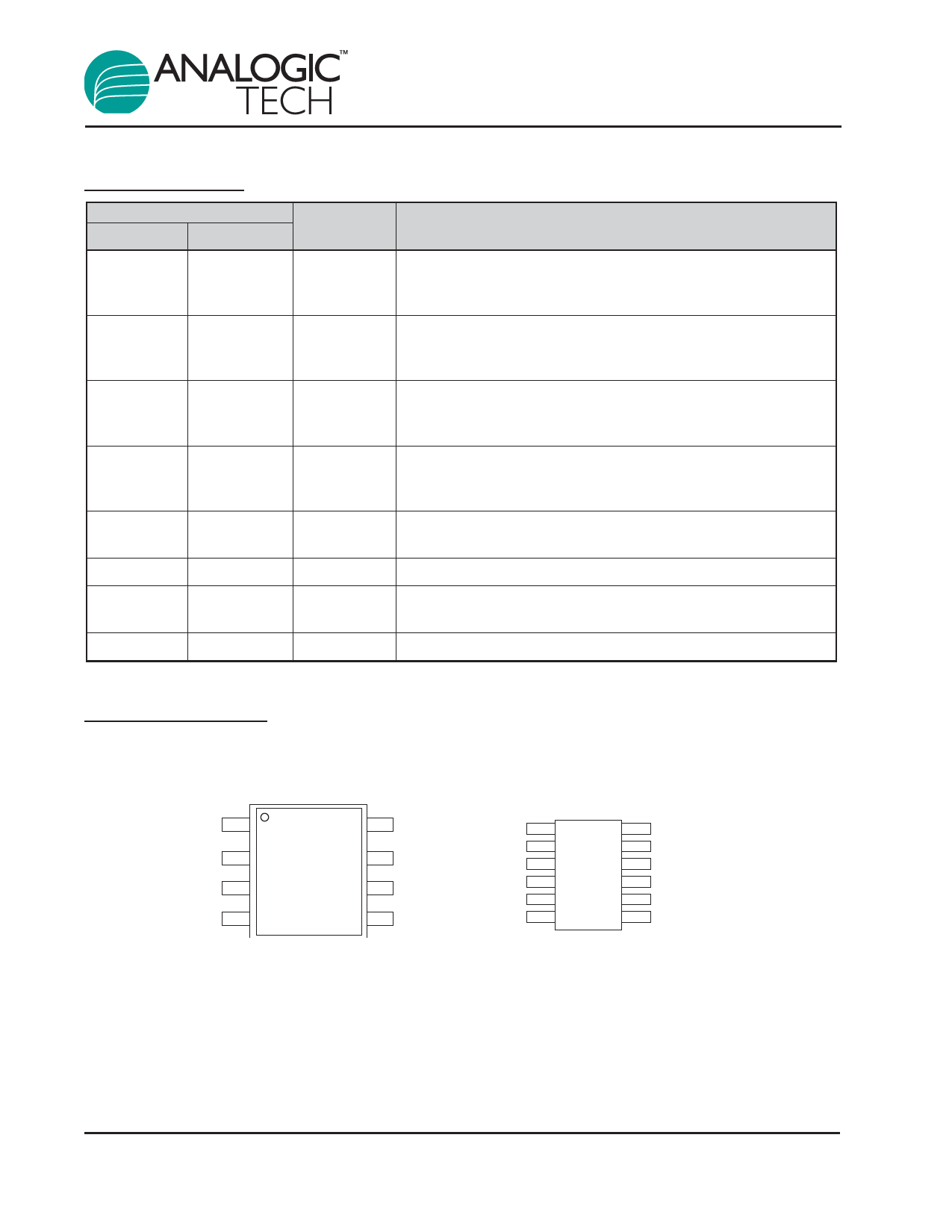
Pin Description
Pin #
MSOP-8
TSOPJW-12
1
5
Symbol
FBP
2
4
EN
3
3
REF
4
2
FBN
5
12
DRVP
6
8, 9, 10, 11
GND
7
7
DRVN
8
1
VIN
Function
Positive charge pump feedback input. Regulates to 1.2V
nominal. Connect feedback resistive divider to analog
ground (GND).
Enable input. When EN is pulled low, the device shuts off
and draws only 1.0µA. When high, it is in normal opera-
tion. Drive EN through an external resistor.
Internal reference bypass terminal. Connect a 0.1µF capac-
itor from this terminal to analog ground (GND). External
load capability to 50µA. REF is disabled in shutdown.
Negative charge pump regulator feedback input. Regulates
to 0V nominal. Connect feedback resistive divider to the
reference (REF).
Positive charge pump driver output. Output high level is VIN
and low level is PGND.
Ground.
Negative charge pump driver output. Output high level is
VIN and low level is PGND.
Input voltage: 2.7V to 5.5V.
Pin Configuration
MSOP-8
(Top View)
TSOPJW-12
(Top View)
FBP 1
EN 2
REF 3
FBN 4
8 VIN
7 DRVN
6 GND
5 DRVP
VIN 1
FBN 2
REF 3
EN 4
FBP 5
N/C 6
12 DRVP
11 GND
10 GND
9 GND
8 GND
7 DRVN
2
3190.2006.01.1.2
Share Link: 