ADSP-21065LKCA-264 データシートの表示(PDF) - Analog Devices
部品番号
コンポーネント説明
一致するリスト
ADSP-21065LKCA-264 Datasheet PDF : 44 Pages
| |||
ADSP-21065L
Pin
SDA10
XTAL
PWM_EVENT1-0
VDD
GND
NC
Type
O/T
O
I/O/A
P
G
Function
SDRAM A10 Pin. Enables applications to refresh an SDRAM in parallel with a host access.
Crystal Oscillator Terminal. Used in conjunction with CLKIN to enable the ADSP-21065L’s
internal clock generator or to disable it to use an external clock source. See CLKIN.
PWM Output/Event Capture. In PWMOUT mode, is an output pin and functions as a timer
counter. In WIDTH_CNT mode, is an input pin and functions as a pulse counter/event capture.
Power Supply; nominally +3.3 V dc. (33 pins)
Power Supply Return. (37 pins)
Do Not Connect. Reserved pins that must be left open and unconnected. (7 pins)
CLOCK SIGNALS
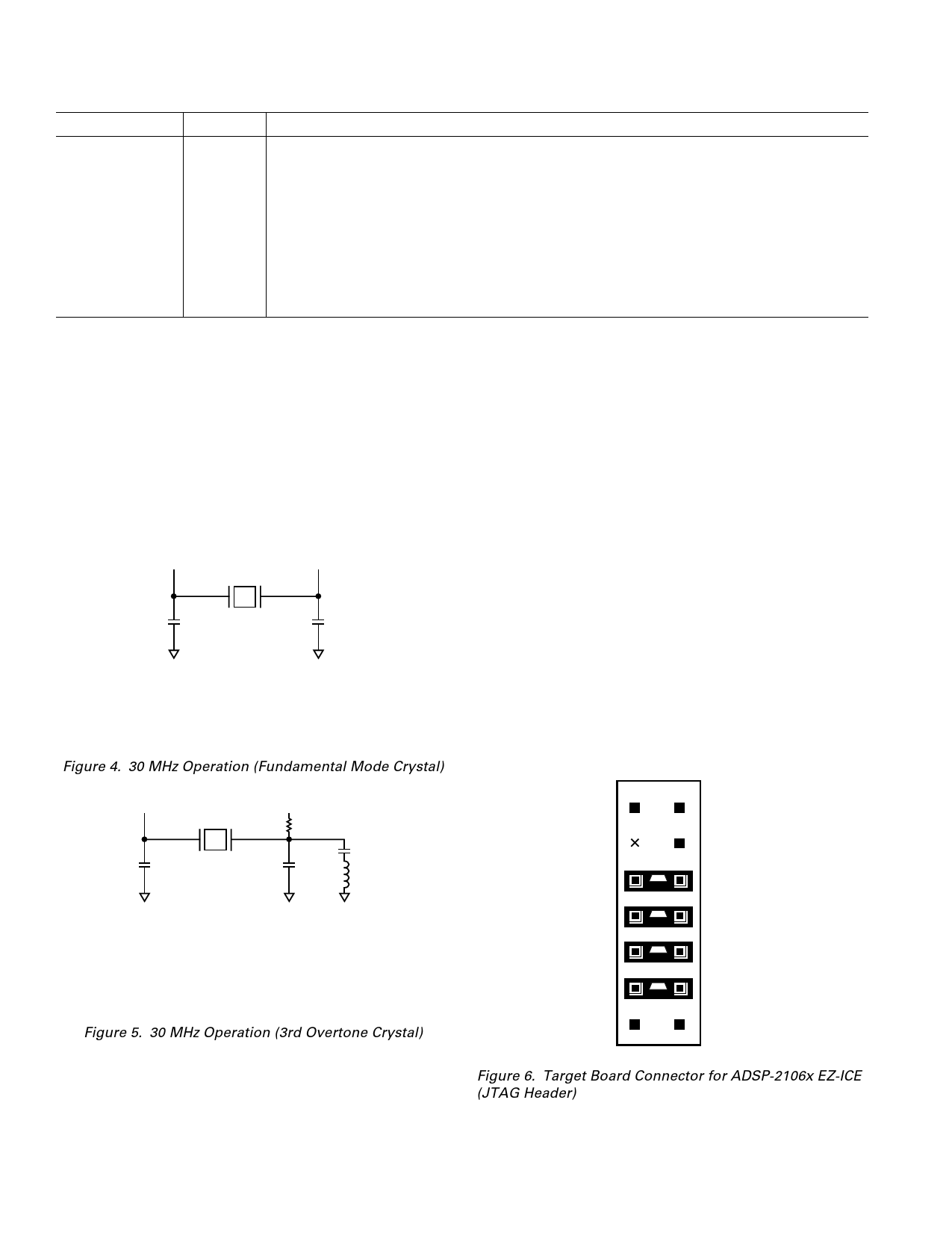
The ADSP-21065L can use an external clock or a crystal. See
CLKIN pin description. You can configure the ADSP-21065L
to use its internal clock generator by connecting the necessary
components to CLKIN and XTAL. You can use either a crystal
operating in the fundamental mode or a crystal operating at an
overtone. Figure 4 shows the component connections used for a
crystal operating in fundamental mode, and Figure 5 shows
the component connections used for a crystal operating at an
overtone.
CLKIN
XTAL
X1
C1
C2
SUGGESTED COMPONENTS FOR 30 MHz OPERATION:
ECLIPTEK EC2SM-33-30.000M (SURFACE MOUNT PACKAGE)
ECLIPTEK EC-33-30.000M (THROUGH-HOLE PACKAGE)
C1 = 33pF
C2 = 27pF
NOTE: C1 AND C2 ARE SPECIFIC TO CRYSTAL SPECIFIED FOR X1.
CONTACT CRYSTAL MANUFACTURER FOR DETAILS.
Figure 4. 30 MHz Operation (Fundamental Mode Crystal)
CLKIN
C1
XTAL
RS
X1
C3
C2
L1
SUGGESTED COMPONENTS FOR 30MHz OPERATION:
ECLIPTEK EC2SM-T-30.000M (SURFACE MOUNT PACKAGE)
ECLIPTEK ECT-30.000M (THROUGH-HOLE PACKAGE)
C1 = 18pF
C2 = 27pF
C3 = 75pF
L1 = 3300nH
RS = SEE NOTE.
NOTE: C1, C2, C3, RS AND L1 ARE SPECIFIC TO CRYSTAL SPECIFIED
FOR X1. CONTACT MANUFACTURER FOR DETAILS.
Figure 5. 30 MHz Operation (3rd Overtone Crystal)
TARGET BOARD CONNECTOR FOR EZ-ICE PROBE
The ADSP-2106x EZ-ICE emulator uses the IEEE 1149.1
JTAG test access port of the ADSP-2106x to monitor and con-
trol the target board processor during emulation. The EZ-ICE
probe requires the ADSP-2106x’s CLKIN, TMS, TCK, TRST,
TDI, TDO, EMU and GND signals be made accessible on the
target system via a 14-pin connector (a 2 row x 7 pin strip header)
such as that shown in Figure 6. The EZ-ICE probe plugs directly
onto this connector for chip-on-board emulation. You must add
this connector to your target board design if you, intend to use
the ADSP-2106x EZ-ICE.
The total trace length between the EZ-ICE connector and the
furthest device sharing the EZ-ICE JTAG pins should be lim-
ited to 15 inches maximum for guaranteed operation. This
restriction on length must include EZ-ICE JTAG signals, which
are routed to one or more 2106x devices or to a combination of
2106xs and other JTAG devices on the chain.
The 14-pin, 2-row pin strip header is keyed at the Pin 3 loca-
tion—you must remove Pin 3 from the header. The pins must
be 0.025 inch square and at least 0.20 inch in length. Pin spac-
ing should be 0.1 ¥ 0.1 inches. Pin strip headers are available
from vendors such as 3M, McKenzie and Samtec.
1
GND
2
EMU
3
KEY (NO PIN)
4
CLKIN (OPTIONAL)
5
6
BTMS
TMS
7
8
BTCK
TCK
9
10
BTRST
9
TRST
11
12
BTDI
TDI
13
GND
14
TDO
TOP VIEW
Figure 6. Target Board Connector for ADSP-2106x EZ-ICE
(JTAG Header)
–10–
REV. C
Share Link: 