CMX631A データシートの表示(PDF) - MX-COM Inc
部品番号
コンポーネント説明
一致するリスト
CMX631A Datasheet PDF : 12 Pages
| |||
Low Voltage SPM Detector
5
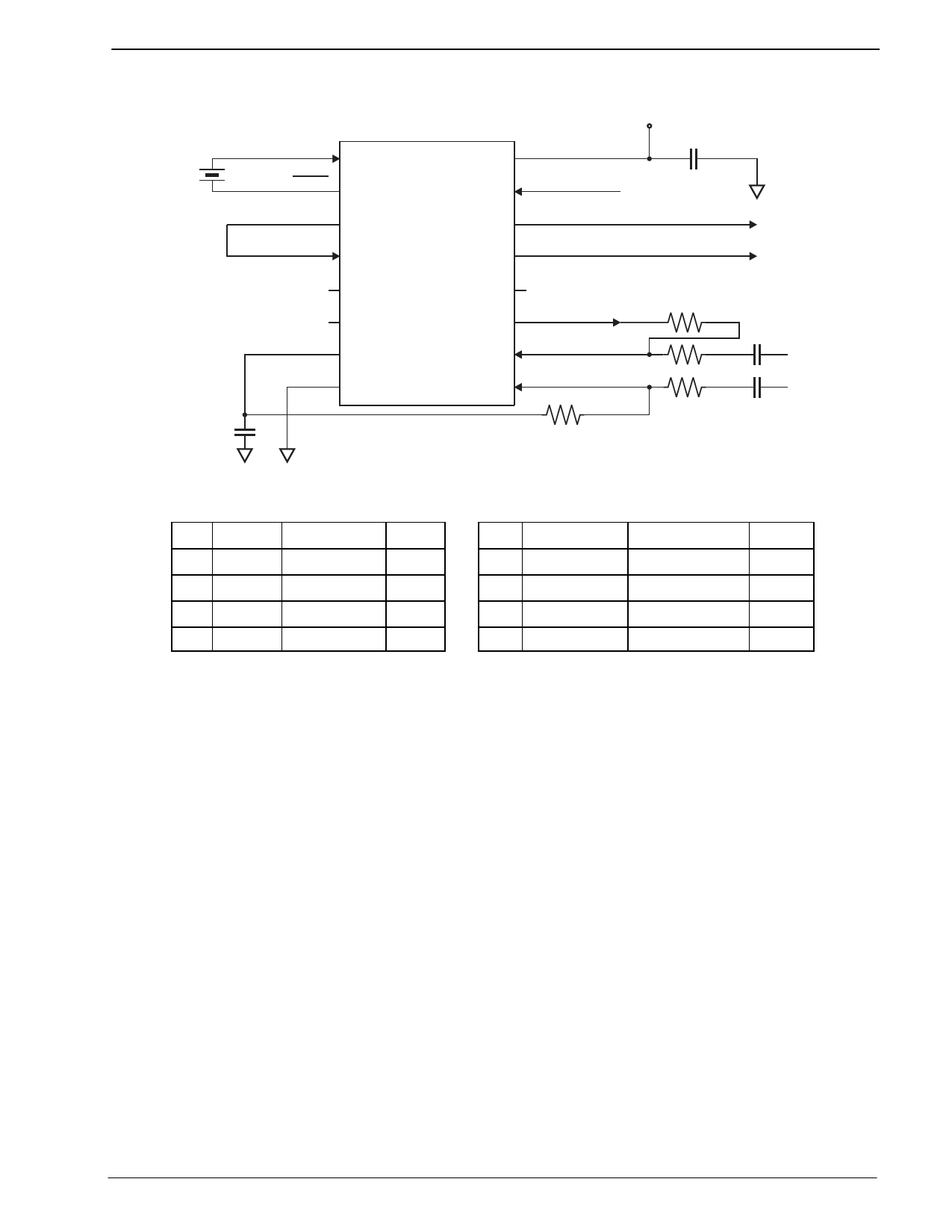
3 External Components
CMX631A PRELIMINARY INFORMATION
XTAL/CLOCK 1
X1
XTAL 2
16 VDD
15 SYSTEM
VDD
C1
CLOCK OUT 3
14 PACKET MODE OUTPUT
CLOCK IN 4
13 TONE FOLLOWER OUTPUT
CMX631A
5 D4/P3 12
6
11 AMP OUT
R1
VBIAS 7
10 SIGNAL IN (-)
R2
C3
VSS 8
9 SIGNAL IN (+)
R3
C4
R4
C2
Figure 2: Recommended External Components
R1 Note 1 RFEEDBACK
R2 Note 1
RIN(-)
R3 Note 1
RIN(+)
R4 Note 1
RBIAS
C1
1.0µF
±20%
C2
1.0µF
±20%
C3
CIN(-)
C4
CIN(+)
X1 Note 2, 3, 4 3.579545MHz
Table 2: Recommended External Components
Recommended External Component Notes:
1. When calculating input gain components, for correct operation R1 and R4 should always be ≥ 33kΩ.
2. For best results, a crystal oscillator design should drive the clock inverter input with signal levels of at
least 40% of VDD, peak to peak. Tuning fork crystals generally cannot meet this requirement. To
obtain crystal oscillator design assistance, consult your crystal manufacturer.
3. The on-chip crystal circuitry includes a feedback resistor (nominally 2MΩ) between pins 1 and 2 and
load capacitors on pins 1 and 2 (nominally 10pF each, excluding package and board parasitics).
4. When using an external clock input, X1 should be removed, Pin 1 (Xtal/Clock) should be tied to VDD,
the Clock In and Clock Out jumper should be removed, and the external clock signal applied to Clock
In.
© 1999 MX•COM Inc.
www.mxcom.com Tele: 800 638-5577 336 744-5050 Fax: 336 744-5054
Doc. # 20480177.004
4800 Bethania Station Road, Winston-Salem, NC 27105-1201 USA All trademarks and service marks are held by their respective companies.
Share Link: 