TC74LCX245F(2010) データシートの表示(PDF) - Toshiba
部品番号
コンポーネント説明
一致するリスト
TC74LCX245F Datasheet PDF : 12 Pages
| |||
TC74LCX245F/FT/FK
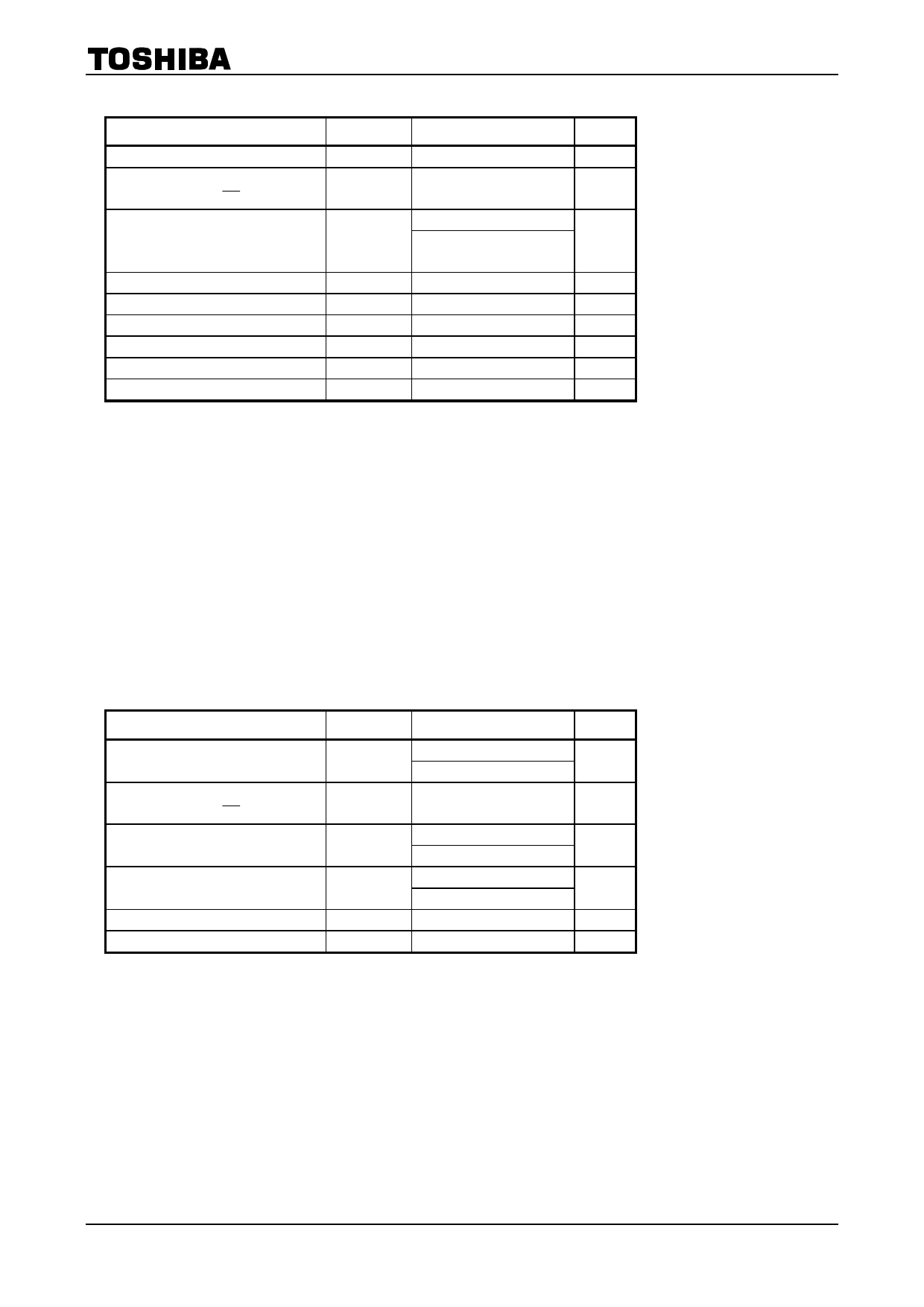
Absolute Maximum Ratings (Note 1)
Characteristics
Power supply voltage
DC input voltage
(DIR, OE )
DC bus I/O voltage
Input diode current
Output diode current
DC output current
Power dissipation
DC VCC/ground current
Storage temperature
Symbol
VCC
VIN
VI/O
IIK
IOK
IOUT
PD
ICC/IGND
Tstg
Rating
Unit
−0.5 to 7.0
V
−0.5 to 7.0
V
−0.5 to 7.0 (Note 2)
−0.5 to VCC + 0.5
V
(Note 3)
−50
mA
±50 (Note 4) mA
±50
mA
180
mW
±100
mA
−65 to 150
°C
Note 1:
Exceeding any of the absolute maximum ratings, even briefly, lead to deterioration in IC performance or
even destruction.
Using continuously under heavy loads (e.g. the application of high temperature/current/voltage and the
significant change in temperature, etc.) may cause this product to decrease in the reliability significantly
even if the operating conditions (i.e. operating temperature/current/voltage, etc.) are within the absolute
maximum ratings and the operating ranges.
Please design the appropriate reliability upon reviewing the Toshiba Semiconductor Reliability Handbook
(“Handling Precautions”/“Derating Concept and Methods”) and individual reliability data (i.e. reliability test
report and estimated failure rate, etc).
Note 2: Output in OFF state
Note 3: High or low state. IOUT absolute maximum rating must be observed.
Note 4: VOUT < GND, VOUT > VCC
Operating Ranges (Note 1)
Characteristics
Power supply voltage
Input voltage
(DIR, OE )
Bus I/O voltage
Output current
Operating temperature
Input rise and fall time
Symbol
VCC
VIN
VI/O
IOH/IOL
Topr
dt/dv
Rating
Unit
1.65 to 3.6
V
1.5 to 3.6 (Note 2)
0 to 5.5
V
0 to 5.5 (Note 3)
0 to VCC (Note 4)
±24 (Note 5)
±12 (Note 6)
−40 to 85
0 to 10 (Note 7)
V
mA
°C
ns/V
Note 1:
The operating ranges are required to ensure the normal operation of the device. Unused inputs and bus
inputs must be tied to either VCC or GND. Please connect both bus inputs and the bus outputs with VCC or
GND when the I/O of the bus terminal changes by the function. In this case, please note that the output is
not short-circuited.
Note 2: Data retention only
Note 3: Output in OFF state
Note 4: High or low state
Note 5: VCC = 3.0 to 3.6 V
Note 6: VCC = 2.7 to 3.0 V
Note 7: VIN = 0.8 to 2.0 V, VCC = 3.0 V
3
2010-01-31
Share Link: 