CY7C1329_04 データシートの表示(PDF) - Cypress Semiconductor
部品番号
コンポーネント説明
一致するリスト
CY7C1329_04 Datasheet PDF : 15 Pages
| |||
CY7C1329
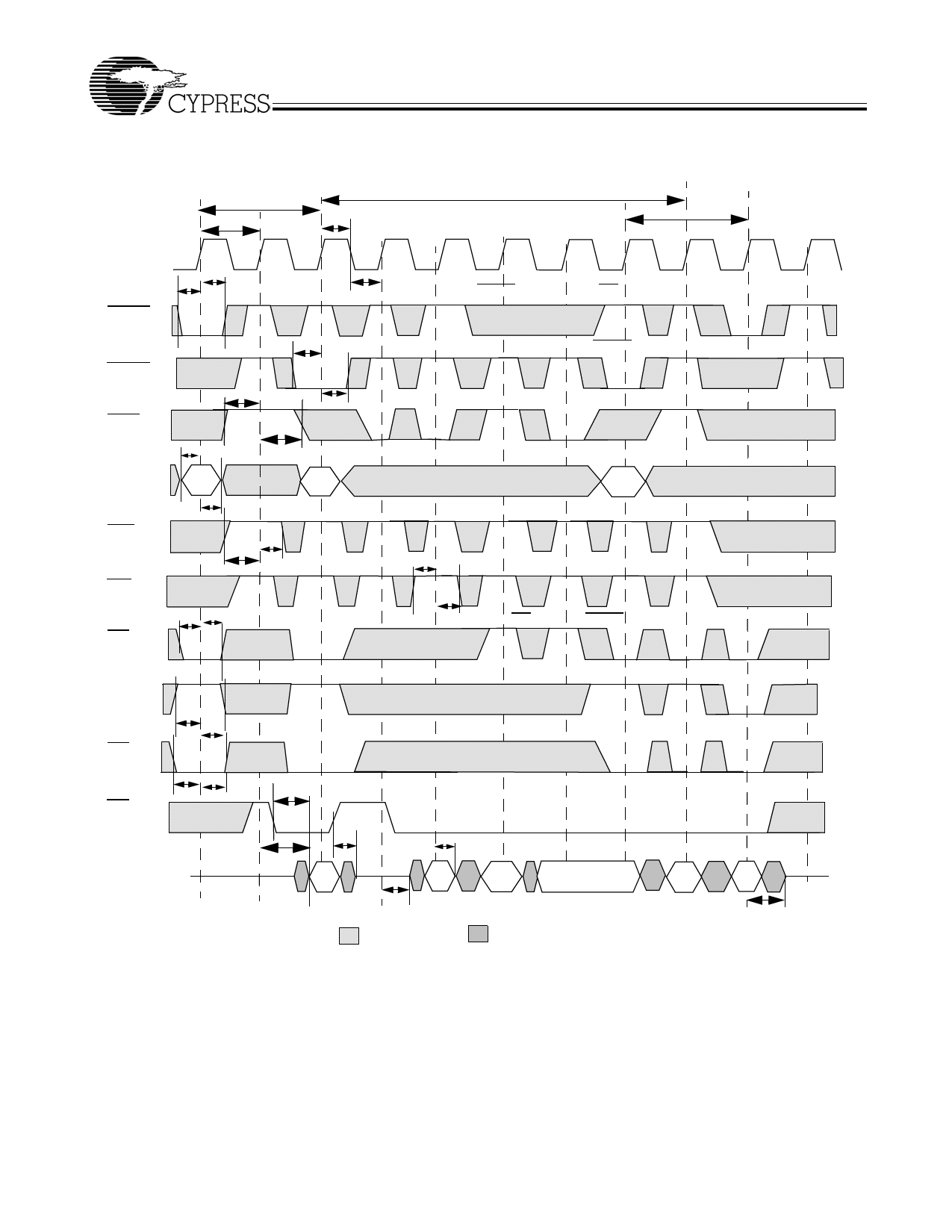
Switching Waveforms (continued)
Read Cycle Timing[14, 16]
CLK
Single Read
tCYC
tCH
Burst Read
Pipelined Read
Unselected
tADS
tADH
tCL
ADSP
ADSC
tADVS
ADV
tAS
ADD
RD1
tADS
tADH
tADVH
RD2
GW
WE
CE1
tAH
tWS
tWH
tCES tCEH
ADSP ignored with CE1 inactive
ADSC initiated Read
Suspend Burst
RD3
tWS
tWH
CE1 masks ADSP
CE2
tCES
CE3
tCES
OE
Data-
Out
tCEH
tCEH
tDOE
tOEHZ
tCO
11aa
tCLZ
tDOH
2a
2b
2c 2c
Note:
16. RDx stands for Read Data from Address X.
= DON’T CARE
= UNDEFINED
Unselected with CE2
2d
3a
tCHZ
Document #: 38-05279 Rev. *B
Page 10 of 15
Share Link: 