CY6264_05 データシートの表示(PDF) - Cypress Semiconductor
部品番号
コンポーネント説明
一致するリスト
CY6264_05 Datasheet PDF : 10 Pages
| |||
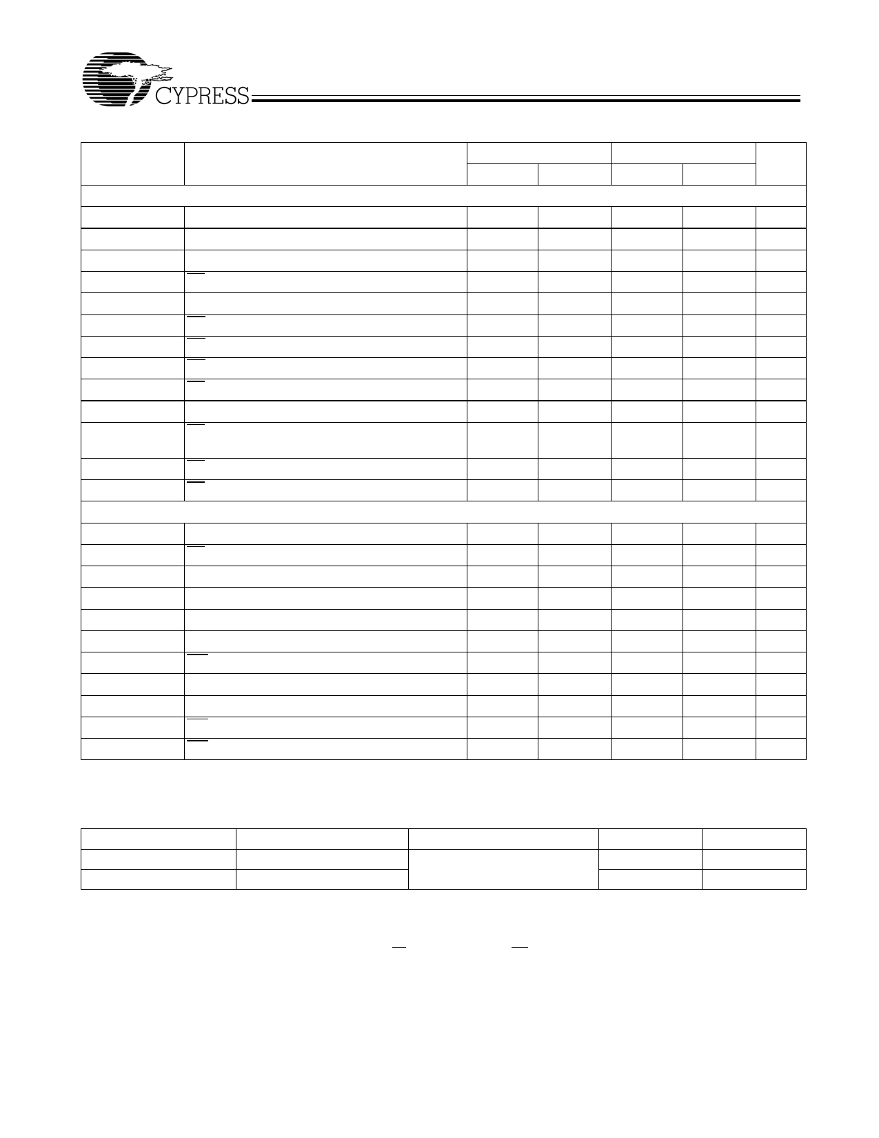
Switching Characteristics Over the Operating Range[3]
Parameter
Description
READ CYCLE
tRC
Read Cycle Time
tAA
Address to Data Valid
tOHA
Data Hold from Address Change
tACE1
CE1 LOW to Data Valid
tACE2
CE2 HIGH to Data Valid
tDOE
OE LOW to Data Valid
tLZOE
tHZOE
tLZCE1
OE LOW to Low Z
OE HIGH to High Z[4]
CE1 LOW to Low Z[5]
tLZCE2
tHZCE
CE2 HIGH to Low Z
CE1 HIGH to High Z[4, 5]
CE2 LOW to High Z
tPU
CE1 LOW to Power-Up
tPD
CE1 HIGH to Power-Down
WRITE CYCLE[6]
tWC
Write Cycle Time
tSCE1
CE1 LOW to Write End
tSCE2
CE2 HIGH to Write End
tAW
Address Set-Up to Write End
tHA
Address Hold from Write End
tSA
Address Set-Up to Write Start
tPWE
WE Pulse Width
tSD
Data Set-Up to Write End
tHD
tHZWE
Data Hold from Write End
WE LOW to High Z[4]
tLZWE
WE HIGH to Low Z
Shaded areas contain advance information.
CY6264
6264-55
Min.
Max.
55
55
5
55
40
25
3
20
5
3
20
0
25
50
40
30
40
0
0
25
25
0
20
5
6264-70
Min.
Max.
Unit
70
ns
70
ns
5
ns
70
ns
70
ns
35
ns
5
ns
30
ns
5
ns
5
ns
30
ns
0
ns
30
ns
70
ns
60
ns
50
ns
55
ns
0
ns
0
ns
40
ns
35
ns
0
ns
30
ns
5
ns
Capacitance[7]
Parameter
Description
Test Conditions
Max.
Unit
CIN
COUT
Input Capacitance
Output Capacitance
TA = 25°C, f = 1 MHz,
VCC = 5.0V
7
pF
7
pF
Notes:
3. Test conditions assume signal transition time of 5 ns or less, timing reference levels of 1.5V, input pulse levels of 0 to 3.0V, and output loading of the specified
IOL/IOH and 30-pF load capacitance.
4. tHZOE, tHZCE, and tHZWE are specified with CL = 5 pF as in part (b) of AC Test Loads. Transition is measured ±500 mV from steady-state voltage.
5. At any given temperature and voltage condition, tHZCE is less than tLZCE for any given device.
6. The internal write time of the memory is defined by the overlap of CE1 LOW, CE2 HIGH, and WE LOW. Both signals must be LOW to initiate a write and either
signal can terminate a write by going HIGH. The data input set-up and hold timing should be referenced to the rising edge of the signal that terminates the write.
7. Tested initially and after any design or process changes that may affect these parameters.
Document #: 001-02367 Rev. **
Page 3 of 10
[+] Feedback
Share Link: 