ISP1562 データシートの表示(PDF) - NXP Semiconductors.
部品番号
コンポーネント説明
一致するリスト
ISP1562 Datasheet PDF : 94 Pages
| |||
NXP Semiconductors
ISP1562
HS USB PCI host controller
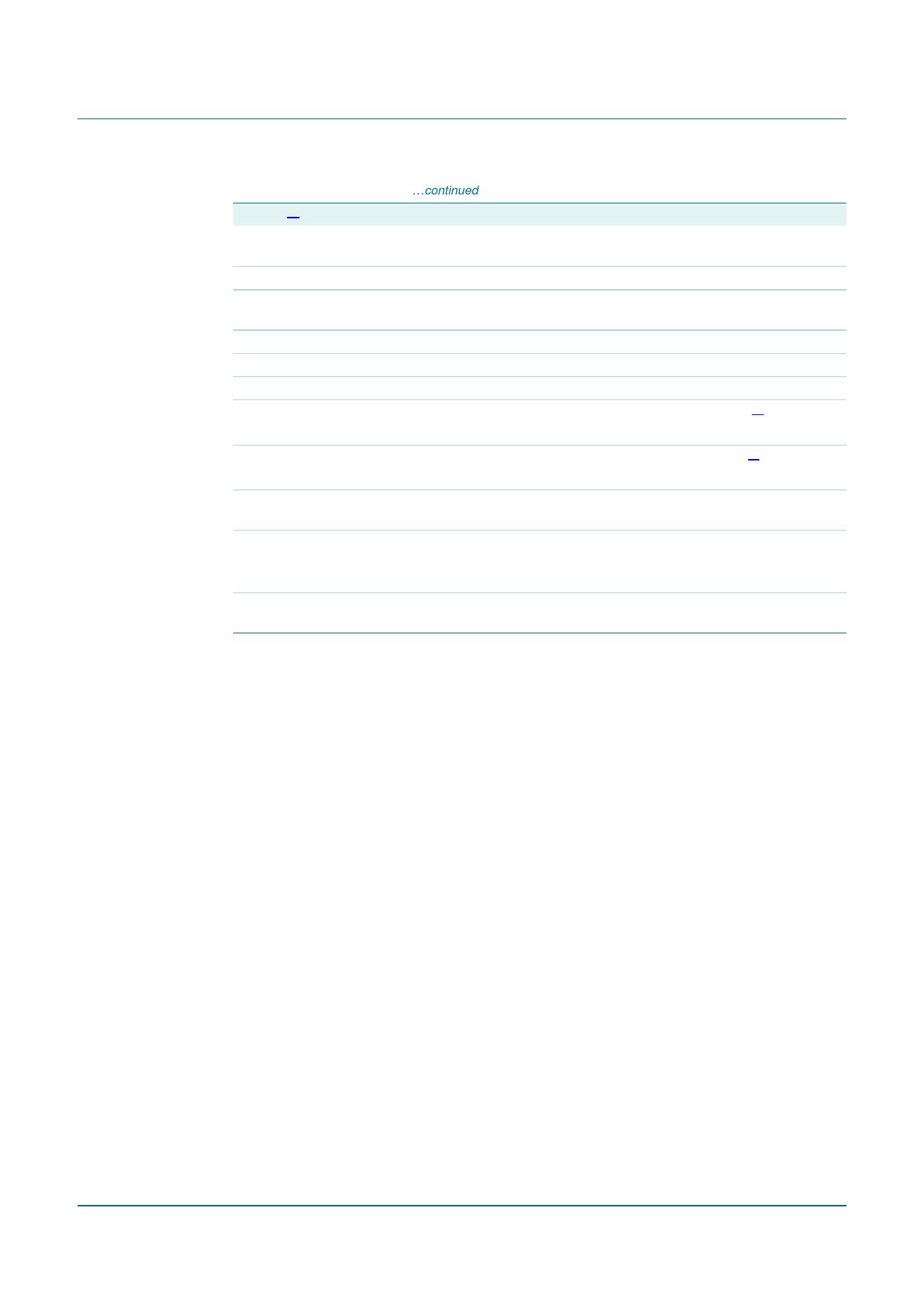
Table 2. Pin description …continued
Symbol[1] Pin Type Description
DM2
90 AI/O D−; analog connection for the USB downstream port 2; pull-down to
ground through a 15 kΩ resistor
GNDA
91 -
analog ground
DP2
92 AI/O D+; analog connection for the USB downstream port 2; pull-down to
ground through a 15 kΩ resistor
VDDA_AUX 93
-
GNDD
94 -
auxiliary analog supply voltage; add a 100 nF decoupling capacitor
digital ground
GNDD
95 -
digital ground
SCL
96 I/O I2C-bus clock; pull-up to 3.3 V through a 10 kΩ resistor[2]
I2C-bus pad; clock signal
SDA
97 I/O I2C-bus data; pull-up to 3.3 V through a 10 kΩ resistor[2]
I2C-bus pad; data signal
VCC(I/O)_AUX 98
-
3.3 V auxiliary supply voltage; used to power pads; add a 100 nF
decoupling capacitor
PME#
99 O
PCI Power Management Event; used by a device to request a
change in the device or system power state
PCI pad; 3.3 V signaling; open-drain
VCC(I/O)_AUX 100 -
3.3 V auxiliary supply voltage; used to power pads; add a 100 nF
decoupling capacitor
[1] Symbol names ending with # represent active LOW signals for PCI pins, for example: NAME#. Symbol
names ending with underscore N represent active LOW signals for USB pins, for example: NAME_N.
[2] Connect to ground if I2C-bus is not used.
ISP1562_3
Product data sheet
Rev. 03 — 14 November 2008
© NXP B.V. 2008. All rights reserved.
9 of 93
Share Link: 