74HCT74 データシートの表示(PDF) - System Logic Semiconductor
部品番号
コンポーネント説明
一致するリスト
74HCT74 Datasheet PDF : 5 Pages
| |||
SL74HCT74
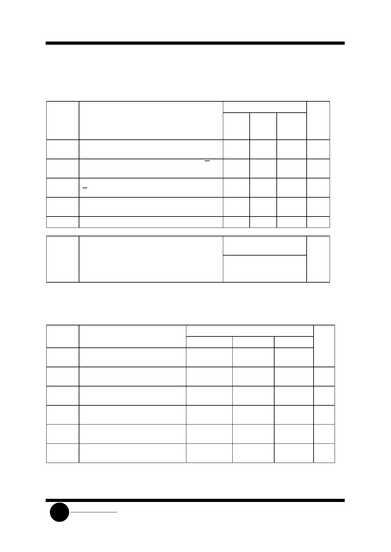
AC ELECTRICAL CHARACTERISTICS(VCC =5.0 V±10%,CL=50pF,Input tr=tf=6.0 ns)
Symbol
Parameter
fmax
tPLH, tPHL
tPLH, tPHL
tTLH, tTHL
CIN
Maximum Clock Frequency (50% Duty Cycle)
(Figures 1 and 4)
Maximum Propagation Delay, Clock to Q or Q
(Figures 1 and 4)
Maximum Propagation Delay, Set or Reset to Q or Q
(Figures 2 and 4)
Maximum Output Transition Time, Any Output
(Figures 1 and 4)
Maximum Input Capacitance
Guaranteed Limit
25 °C
to
-55°C
≤85°C ≤125°C
30
24
20
24
30
36
24
30
36
15
19
22
10
10
10
Unit
MHz
ns
ns
ns
pF
Power Dissipation Capacitance (Per Enabled
Output)
CPD Used to determine the no-load dynamic power
consumption:
PD=CPDVCC2f+ICCVCC
Typical @25°C,VCC=5.0 V
130
pF
TIMING REQUIREMENTS(VCC =5.0 V±10%,CL=50pF,Input tr=tf=6.0 ns)
Guaranteed Limit
Symbol
Parameter
25 °C to-55°C
≤85°C
≤125°C Unit
tsu
Minimum Setup Time, Data to Clock
15
(Figure 3)
19
22
ns
th
Minimum Hold Time, Clock to Data
3
(Figure 3)
3
3
ns
trec
Minimum Recovery Time, Set or Reset
6
Inactive to Clock (Figure 2)
8
9
ns
tw
Minimum Pulse Width, Clock (Figure
15
1)
19
22
ns
tw
Minimum Pulse Width, Set or Reset
15
(Figure 2)
19
22
ns
tr, tf Maximum Input Rise and Fall Times
500
(Figure 1)
500
500
ns
SLS
System Logic
Semiconductor
Share Link: 