74HCT74 データシートの表示(PDF) - System Logic Semiconductor
部品番号
コンポーネント説明
一致するリスト
74HCT74 Datasheet PDF : 5 Pages
| |||
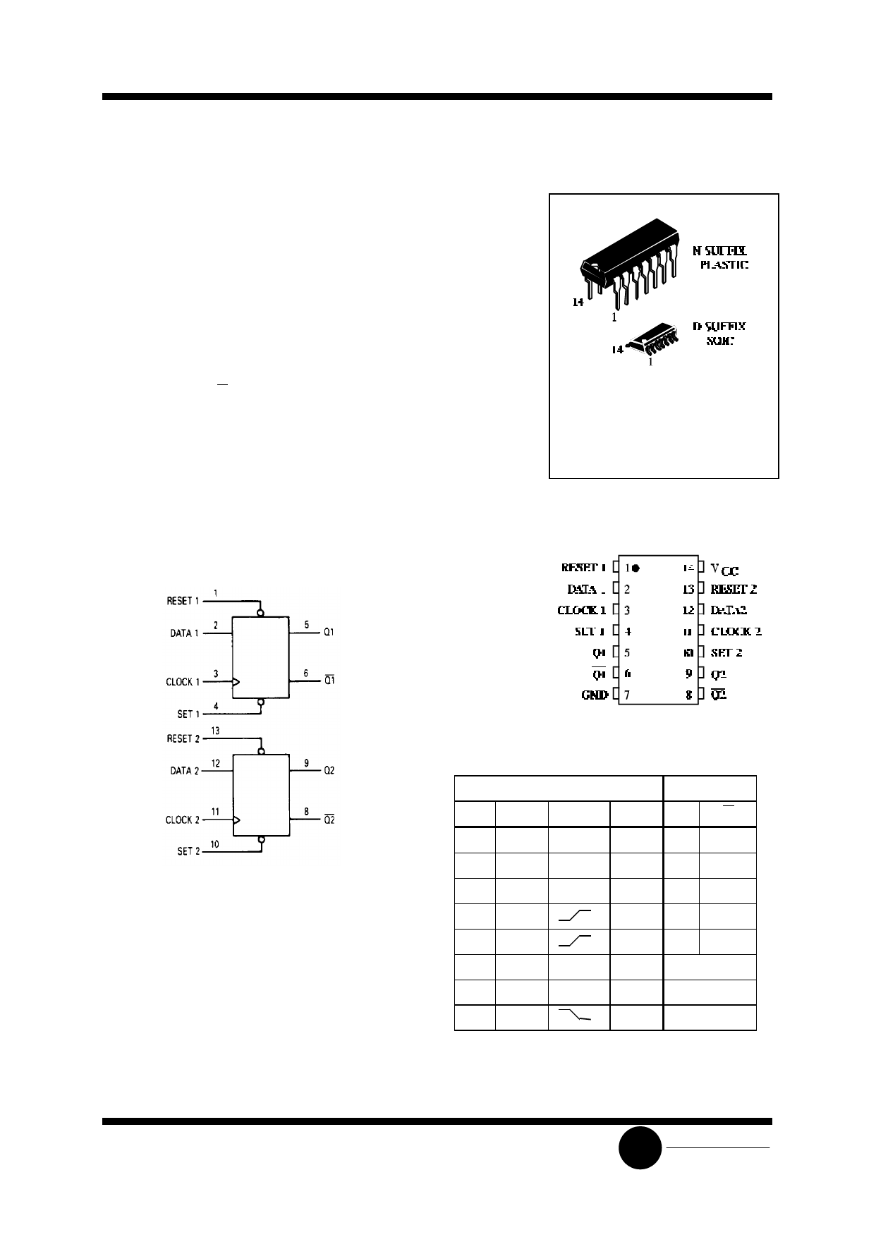
SL74HCT74
Dual D Flip-Flop with Set and Reset
High-Performance Silicon-Gate CMOS
The SL74HCT74 is identical in pinout to the LS/ALS74. This device
may be used as a level converter for interfacing TTL or NMOS outputs
to High Speed CMOS inputs.
This device consists of two D flip-flops with individual Set, Reset,
and Clock inputs. Information at a D-input is transferred to the
corresponding Q output on the next positive going edge of the clock
input. Both Q and Q outputs are available from each flip-flop. The Set
and Reset inputs are asynchronous.
• TTL/NMOS Compatible Input Levels
• Outputs Directly Interface to CMOS, NMOS, and TTL
• Operating Voltage Range: 4.5 to 5.5 V
• Low Input Current: 1.0 µA
ORDERING INFORMATION
SL74HCT74N Plastic
SL74HCT74D SOIC
TA = -55° to 125° C for all packages
LOGIC DIAGRAM
PIN ASSIGNMENT
PIN 14 =VCC
PIN 7 = GND
FUNCTION TABLE
Inputs
Outputs
Set Reset Clock Data Q Q
L
H
X
XH L
H
L
X
XLH
L
L
X
X
H*
H*
H
H
HH L
H
H
LLH
H
H
L
X No Change
H
H
H
X No Change
H
H
X No Change
*Both outputs will remain high as long as Set and
Reset are low, but the output states are
unpredictable if Set and Reset go high
simultaneously.
X = don’t care
SLS
System Logic
Semiconductor
Share Link: 