UPD720102 データシートの表示(PDF) - NEC => Renesas Technology
部品番号
コンポーネント説明
一致するリスト
UPD720102 Datasheet PDF : 36 Pages
| |||
μPD720102
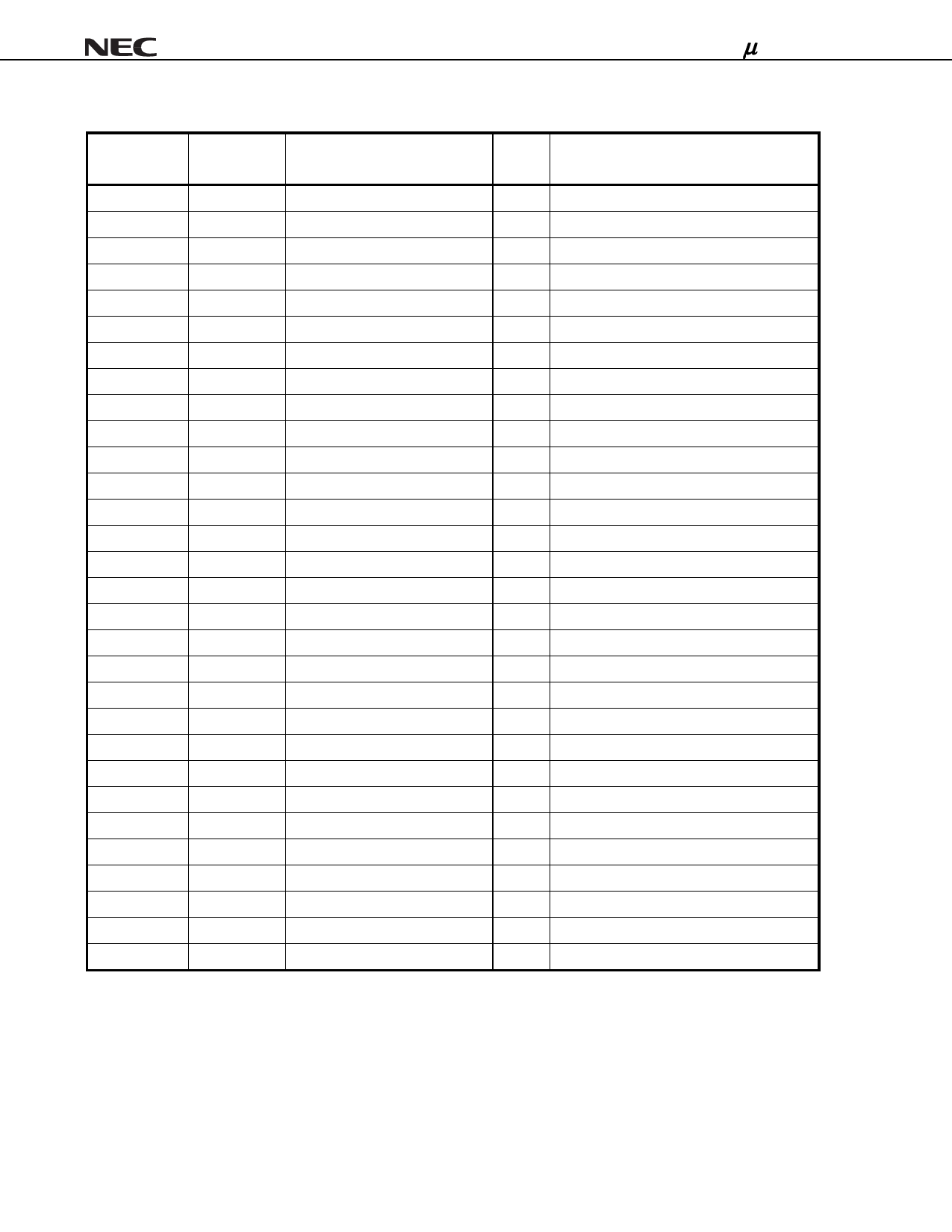
1. PIN INFORMATION
Pin Name
I/O
Normal (Test)
Buffer Type
Active
Level
Function
(1/2)
AD (31:0)
I/O
3.3 V PCI I/O with OR input
PCI “AD [31:0]” signal
CBE (3:0)0
I/O
3.3 V PCI I/O with OR input
PCI “C/BE [3:0]” signal
PAR
I/O
3.3 V PCI I/O with OR input
PCI “PAR” signal
FRAME0
I/O
3.3 V PCI I/O with OR input
Low
PCI “FRAME#” signal
IRDY0
I/O
3.3 V PCI I/O with OR input
Low
PCI “IRDY#” signal
TRDY0
I/O
3.3 V PCI I/O with OR input
Low
PCI “TRDY#” signal
STOP0
I/O
3.3 V PCI I/O with OR input
Low
PCI “STOP#” signal
IDSEL
I
3.3 V PCI input with OR input
High
PCI “IDSEL” signal
DEVSEL0
I/O
3.3 V PCI I/O with OR input
Low
PCI “DEVSEL#” signal
REQ0
O (I/O)
3.3 V PCI I/O with OR input
Low
PCI “REQ#” signal
GNT0
I
3.3 V PCI input with OR input
Low
PCI “GNT#” signal
PERR0
SERR0
INTA0
I/O
O (I/O)
O (I/O)
3.3 V PCI I/O with OR input
Low
3.3 V PCI I/O with OR input Note 1
Low
3.3 V PCI I/O with OR input Note 1
Low
PCI “PERR#” signal
PCI “SERR#” signal
PCI “INTA#” signal
PCLK
I
3.3 V PCI input with OR input
PCI “CLK” signal
VBBRST0
I
3.3 V schmitt input
Low
PCI “RST#” signal
CRUN0
I/O
3.3 V PCI I/O with OR input
Low
PCI “CLKRUN#” signal
PME0
O
N-ch open drain buffer
Low
PCI “PME#” signal
VCCRST0
I
3.3 V schmitt input
Low
PCI “RST#” signal for D3cold support
SMI0
O (I/O)
3.3 V I/O buffer
Low
System management interrupt output
XT1/SCLK
I
OSC block
System clock input or oscillator in
XT2
O
OSC block
Oscillator out
CLKSEL
I
3.3 V Input
Input clock frequency select signal
HSMODE
I
3.3 V Input
High
Hyper-Speed transfer mode enable signal
SRCLK
O (I/O)
3.3 V I/O buffer
Serial ROM clock out
SRDTA
I/O
3.3 V I/O buffer
Serial ROM data
SRMOD
TESTEN Note 2
TEST3 Note 2
TEST4 Note 2
I
3.3 V Input with pull down resistor High Serial ROM input enable
I
3.3 V Input with pull down resistor High Test enable pin
I
3.3 V Input with pull down resistor High
Test control
I
3.3 V Input with pull down resistor High
Test control
Notes 1. These signals become N-ch open drain buffers in normal operation.
2. These pins must be open on board.
8
Data Sheet S17998EJ4V0DS
Share Link: 