UPD720102 データシートの表示(PDF) - NEC => Renesas Technology
部品番号
コンポーネント説明
一致するリスト
UPD720102 Datasheet PDF : 36 Pages
| |||
μPD720102
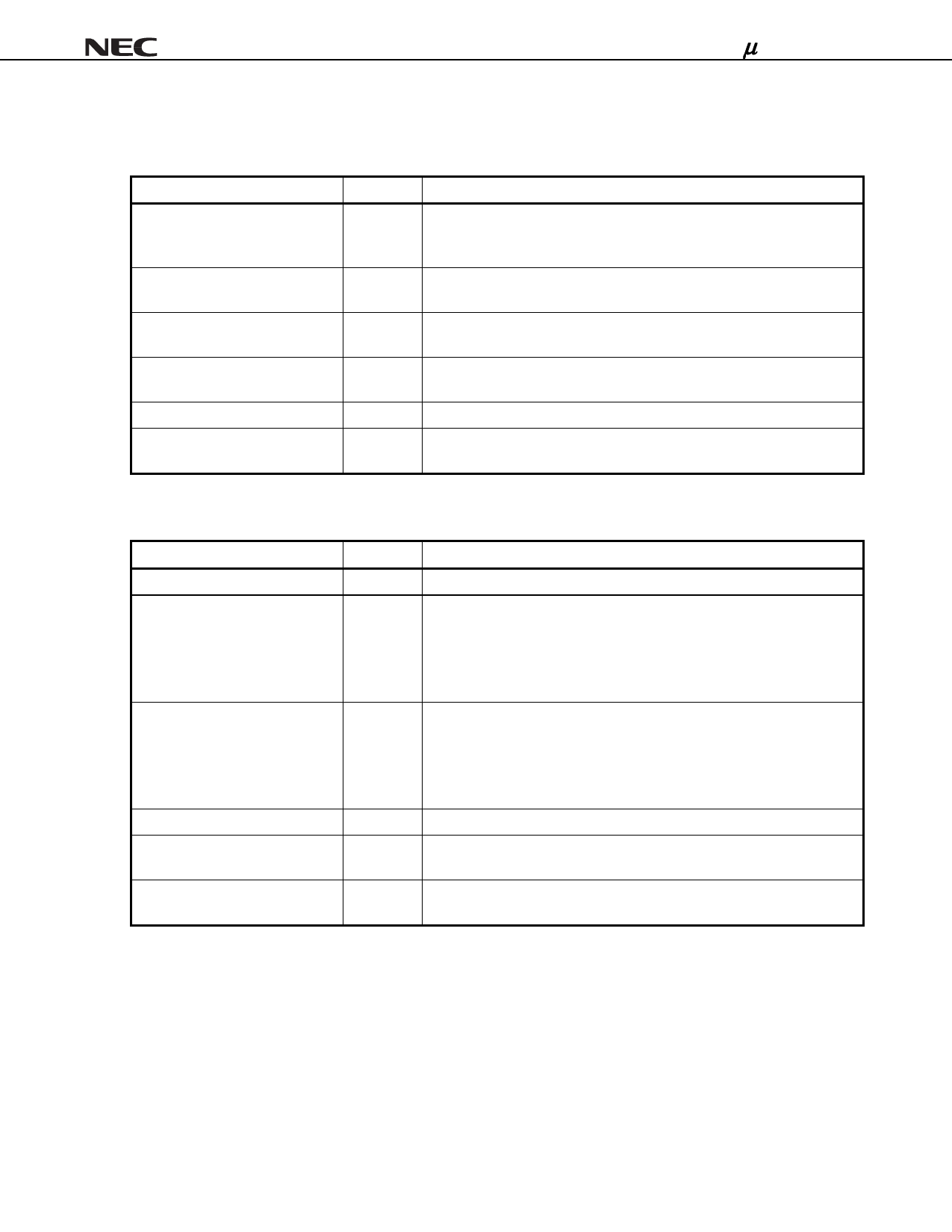
3.2 Terminology
Terms Used in Absolute Maximum Ratings
Parameter
Power supply voltage
Input voltage
Output voltage
Output current
Operating ambient temperature
Storage temperature
Symbol
VDD, VDD15,
AVDD33,
AVDD15
VI
VO
IO
TA
Tstg
Meaning
Indicates the voltage range within which damage or reduced reliability will not
result when power is applied to a VDD pin.
Indicates voltage range within which damage or reduced reliability will not
result when power is applied to an input pin.
Indicates voltage range within which damage or reduced reliability will not
result when power is applied to an output pin.
Indicates absolute tolerance values for DC current to prevent damage or
reduced reliability when current flows out of or into output pin.
Indicates the ambient temperature range for normal logic operations.
Indicates the element temperature range within which damage or reduced
reliability will not result while no voltage or current is applied to the device.
Terms Used in Recommended Operating Range
Parameter
Power supply voltage
High-level input voltage
Low-level input voltage
Hysteresis voltage
Input rise time
Input fall time
Symbol
Meaning
VDD, AVDD33 Indicates the voltage range for normal logic operations occur when VSS = 0 V.
VIH
Indicates the voltage, which is applied to the input pins of the device, is the
voltage indicates that the high level states for normal operation of the input
buffer.
* If a voltage that is equal to or greater than the “Min.” value is applied, the
input voltage is guaranteed as high level voltage.
VIL
Indicates the voltage, which is applied to the input pins of the device, is the
voltage indicates that the low level states for normal operation of the input
buffer.
* If a voltage that is equal to or lesser than the “Max.” value is applied, the
input voltage is guaranteed as low level voltage.
VH
Indicates the differential between the positive and the negative trigger voltage.
tri
Indicates allowable input rise time to input signal transition time from 0.1 x VDD
to 0.9 x VDD.
tfi
Indicates allowable input fall time to input signal transition time from 0.9 x VDD
to 0.1 x VDD.
Data Sheet S17998EJ4V0DS
15
Share Link: 