ADG528A データシートの表示(PDF) - Analog Devices
部品番号
コンポーネント説明
一致するリスト
ADG528A Datasheet PDF : 12 Pages
| |||
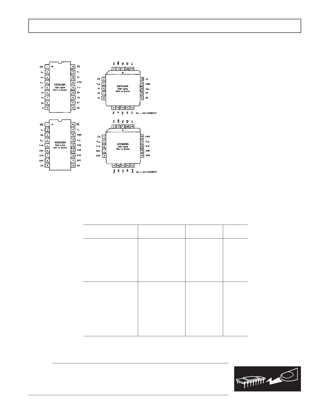
PIN CONFIGURATIONS
DIP/SOIC
PLCC
ADG528A/ADG529A
ABSOLUTE MAXIMUM RATINGS1
(TA = +25°C, unless otherwise noted)
VDD to VSS . . . . . . . . . . . . . . . . . . . . . . . . . . . . . . . . . . . . . 44 V
VDD to GND . . . . . . . . . . . . . . . . . . . . . . . . . . . . . . . . . . . 25 V
VSS to GND . . . . . . . . . . . . . . . . . . . . . . . . . . . . . . . . . . . –25 V
Analog Inputs2
Voltage at S, D . . . . . . . . . VSS – 2 V to VDD + 2 V or 20 mA,
whichever Occurs First
Continuous Current, S or D . . . . . . . . . . . . . . . . . . . 20 mA
Pulsed Current, S or D
1 ms duration, 10% Duty Cycle . . . . . . . . . . . . . . . 40 mA
Digital Inputs1
Voltage at A, EN, WR, RS . . . . . . VSS – 4 V to VDD + 4 V or
20 mA, whichever Occurs First
Power Dissipation (Any Package)
Up to +75°C . . . . . . . . . . . . . . . . . . . . . . . . . . . . . . 470 mW
Derates above +75°C . . . . . . . . . . . . . . . . . . . . . . . 6 mW/°C
Operating Temperature
Commercial (K Version) . . . . . . . . . . . . . . . –40°C to +85°C
Industrial (B Version) . . . . . . . . . . . . . . . . . –40°C to +85°C
Extended (T Version) . . . . . . . . . . . . . . . . –55°C to +125°C
Storage Temperature Range . . . . . . . . . . . . . –65°C to +150°C
Lead Temperature (Soldering, 10 sec) . . . . . . . . . . . . +300°C
NOTES
1Stresses above those listed under “Absolute Maximum Ratings” may cause permanent
damage to the device. This is a stress rating only and functional operation of the device
at these or any other conditions above those indicated in the operational sections of this
specification is not implied. Exposure to absolute maximum rating conditions for
extended periods may affect device reliability.
2Overvoltage at A, EN, WR, RS, S or D will be clamped by diodes. Current should
be limited to the maximum rating above.
ORDERING GUIDE
Model
Temperature
Range
Package
Description
Package
Option1
ADG528AKN
ADG528AKP
ADG528AKP-REEL
ADG528ABQ
ADG528ATQ
ADG528ABCHIPS
ADG528ATCHIPS
–40°C to +85°C
–40°C to +85°C
–40°C to +85°C
–40°C to +85°C
–55°C to +125°C
PDIP
PLCC
PLCC
CERDIP
CERDIP
DIE
DIE
N-18
P-20A
P-20A
Q-18
Q-18
ADG529AKN
ADG529AKP
ADG529AKRW
ADG529AKRW-REEL
ADG529AKRW-REEL7
ADG529ABQ
ADG529ATQ
ADG529ABCHIPS
ADG529ATCHIPS
–40°C to +85°C
–40°C to +85°C
–40°C to +85°C
–40°C to +85°C
–40°C to +85°C
–40°C to +85°C
–55°C to +125°C
PDIP
PLCC
SOIC
SOIC
SOIC
CERDIP
CERDIP
DIE
DIE
N-18
P-20A
RW-18
RW-18
RW-18
Q-18
Q-18
NOTES
1N = Plastic DIP; P = Plastic Leaded Chip Carrier (PLCC); Q = Cerdip; RW = SOIC.
CAUTION
ESD (electrostatic discharge) sensitive device. Electrostatic charges as high as 4000 V readily
accumulate on the human body and test equipment and can discharge without detection. Although the
ADG528A/ADG529A features proprietary ESD protection circuitry, permanent damage may occur
on devices subjected to high energy electrostatic discharges. Therefore, proper ESD precautions are
recommended to avoid performance degradation or loss of functionality.
REV. B
–5–
WARNING!
ESD SENSITIVE DEVICE
Share Link: 