HIP1011D データシートの表示(PDF) - Intersil
部品番号
コンポーネント説明
一致するリスト
HIP1011D Datasheet PDF : 15 Pages
| |||
HIP1011D, HIP1011E
TABLE 1.
HOW TO DETERMINE +25c NOMINAL (±10%) IOC
SUPPLY
FOR EACH SUPPLY
+3.3V IOC
+5.0V IOC
+12V IOC
-12V IOC
((100µA x ROCSET)/11.5)/RRSENSE
((100µA x ROCSET)/14.5)/RRSENSE
(100µA x ROCSET)/1
(100µA x ROCSET)/3.4
Time Delay to Latch-Off
Time delay to latch-off allows for a predetermined delay from
an OC or UV in the HIP1011D or an OC in the HIP1011E
event to the simultaneous latch-off of all four supply switches
of the affected slot. This delay period is set by the
capacitance value to ground from the FLTN pins for each
slot. This capacitance value tailors the FLTN signal going low
ramp rate. This provides a delay to the fault signal latch-off
threshold voltage, FLTN, Vth. By increasing this time, the
HIP1011D/E delays immediate latch-off of the bus supply
switches, thus ignoring transient faults. See additional
information in the “Using the HIP1011DEVAL1 Platform”
section of this data sheet. The HIP1011E has all features of
the HIP1011D but it does not respond to UV events.
Caution: The primary purpose of a protection device such
as the HIP1011D/E is to quickly isolate a faulted card from
the voltage bus. Delaying the time to latch-off works against
this primary concern so care must be taken when using this
feature. Ensure adequate sizing of external FETs to carry
additional current during time out period. Understand that
voltage bus disruptions must be minimized for the time delay
period in the event of a crow bar failure.
Devices using an unadjustable preset delay to latch-off time
present the user with the inability to eliminate these
concerns increasing cost and the chance of additional ripple
through failures.
HIP1011D, HIP1011E Soft Start and Turn-Off
Considerations
The HIP1011D/E does allow the user to select the rate of
ramp up on the voltage supplies. This startup ramp
minimizes in-rush current at startup while the on card bulk
capacitors charge. The ramp is created by placing
capacitors on M12VG to M12VO, 12VG to 12VO and 3V5VG
to ground. These capacitors are each charged up by a
nominal 25µA current during turn on. The same value for all
gate timing capacitors is recommended. A recommended
minimum value of 0.033µF as a smaller value may cause
overcurrent faults at power up. This recommendation results
in a nominal gate voltage ramp rate of 0.76V/ms. The gate
capacitors must be discharged when a fault is detected to
turn off the power FETs. Thus, larger caps slow the response
time. If the gate capacitors are too large the HIP1011D/E
may not be able to adequately protect the bus or the power
FETs. The HIP1011D/E have internal discharge FETs to
discharge the load when disabled. Upon turn-off these
internal switches on each output discharge the load
capacitance pulling the output to GND. These switches are
also on when PWRON is low thus an open slot is held at the
GND level.
Decoupling Precautions and Recommendations
For the HIP1011D/E proper decoupling is a particular
concern during the normal switching operation and
especially during a card crowbar failure. If a card
experiences a crow bar short to ground, the supply to the
other card will experience transients until the faulted card is
isolated from the bus. In addition the common IC nodes
between the two sides can fluctuate unpredictably resulting
in a false latch-off of the second slot. Additionally to the
mother board bulk capacitance, it is recommended that 10µF
capacitors be placed on both the +12V and -12V lines of the
HIP1011D/E as close to the chip as possible.
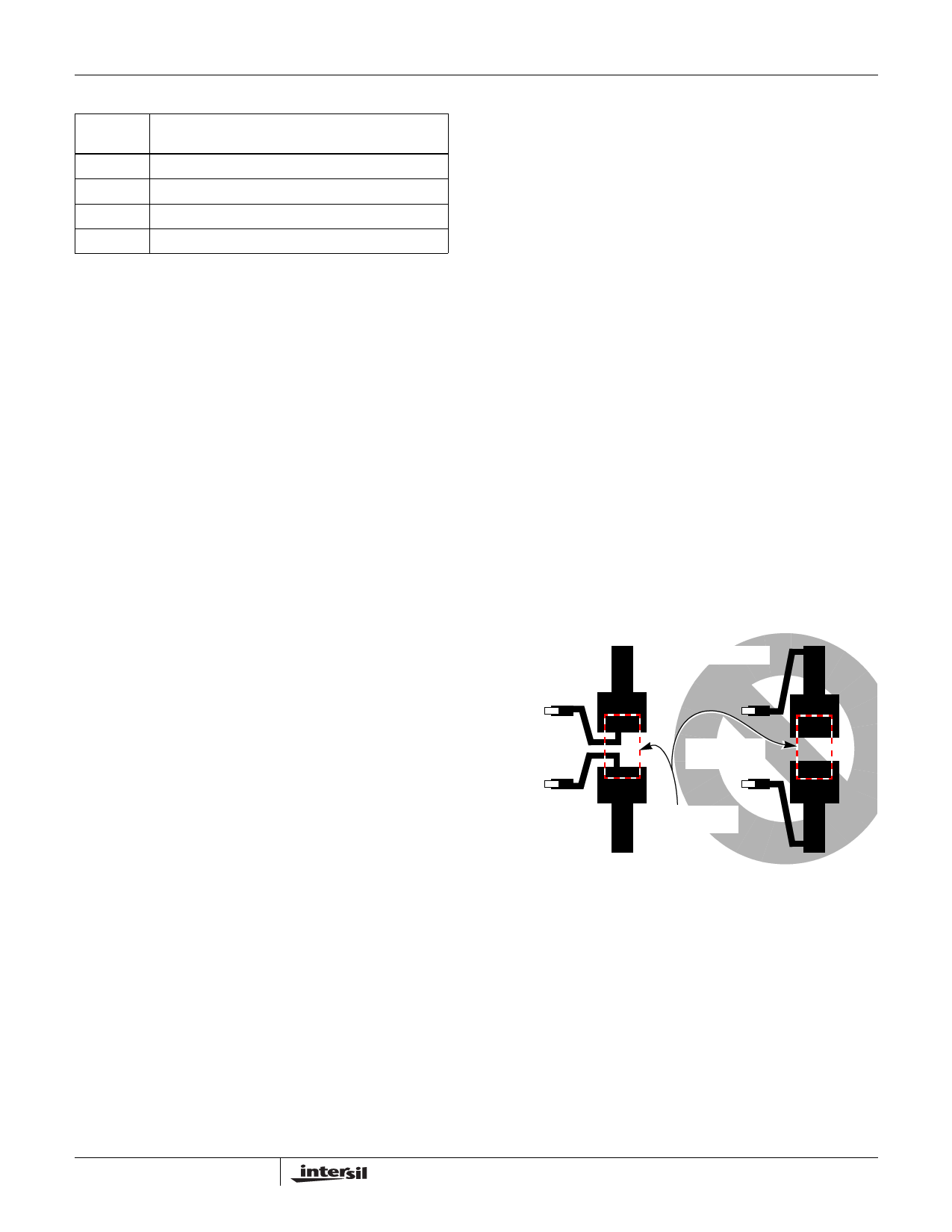
Recommended PCB Layout Design Best Practices
To ensure accurate current sensing, PCB traces that
connect each of the current sense resistors to the
HIP1011D/E must not carry any load current. This can be
accomplished by two dedicated PCB kelvin traces directly
from the sense resistors to the HIP1011D/E (see examples
of correct and incorrect layouts below in Figure 3). To reduce
parasitic inductance and resistance effects, maximize the
width of the high-current PCB traces.
CORRECT
INCORRECT
TO HIP1011D/E
VS AND VISEN
TO HIP1011D
VS AND VISEN
CURRENT
SENSE RESISTOR
FIGURE 3. SENSE RESISTOR PCB LAYOUT
8
FN4725.5
November 18, 2004
Share Link: 