HFA3861B データシートの表示(PDF) - Intersil
部品番号
コンポーネント説明
一致するリスト
HFA3861B Datasheet PDF : 36 Pages
| |||
HFA3861B
Power Down Modes
The power consumption modes of the HFA3861B are
controlled by the following control signals.
Receiver Power Enable (RX_PE, pin 61), which disables the
receiver when inactive.
Transmitter Power Enable (TX_PE, pin 62), which disables
the transmitter when inactive.
Reset (RESET, pin 63), which puts the receiver in a sleep
mode. The power down mode where, both RESET and
RX_PE are used is the lowest possible power consumption
mode for the receiver. Exiting this mode requires a
maximum of 10µs before the device is operational.
The contents of the Configuration Registers are not effected
by any of the power down modes. No reconfiguration is
required when returning to operational modes. Activation of
RESET does corrupt learned values of AGC settings and
noise floor values. Optimum receiver operation may not be
achieved until these values are reestablished (typically
<50µs of operation in noise only needed). The power
savings of activating RESET must be weighed against this.
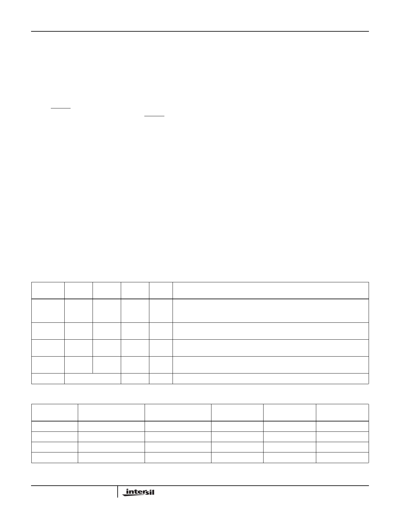
Table 2 describes the power down modes available for the
HFA3861B (VCC = 3.3V). The table values assume that all
other inputs to the part (MCLK, SCLK, etc.) continue to run
except as noted.
Transmitter Description
The HFA3861B transmitter is designed as a Direct
Sequence Spread Spectrum Phase Shift Keying (DSSS
PSK) modulator. It can handle data rates of up to 11Mbps
(refer to AC and DC specifications). The various modes of
the modulator are Differential Binary Phase Shift Keying
(DBPSK) for 1Mbps, Differential Quaternary Phase Shift
Keying (DQPSK) for 2Mbps, and Complementary Code
Keying (CCK) for 5.5Mbps and 11Mbps. These implement
data rates as shown in Table 3. The major functional blocks
of the transmitter include a network processor interface,
DPSK modulator, high rate modulator, a data scrambler and
a spreader, as shown in Figure 7. CCK is essentially a
quadra-phase form of M-ARY Orthogonal Keying. A
description of that modulation can be found in Chapter 5 of:
“Telecommunications System Engineering”, by Lindsey and
Simon, Prentis Hall publishing.
The preamble is always transmitted as the DBPSK
waveform while the header can be configured to be either
DBPSK, or DQPSK, and data packets can be configured for
DBPSK, DQPSK, or CCK. The preamble is used by the
receiver to achieve initial PN synchronization while the
header includes the necessary data fields of the
communications protocol to establish the physical layer
link. The transmitter generates the synchronization
preamble and header and knows when to make the DBPSK
to DQPSK or CCK switchover, as required.
MODE
SLEEP
RX_PE
Inactive
TX_PE
Inactive
STANDBY Inactive Inactive
TX
Inactive Active
RX
Active Inactive
NO CLOCK
ICC Standby
RESET
Active
Inactive
Inactive
Inactive
Active
TABLE 2. POWER DOWN MODES
AT
44MHz
DEVICE STATE
1mA
Both transmit and receive functions disabled. Device in sleep mode. Control
Interface is still active. Register values are maintained. Device will return to its active
state within 10µs.
1.5mA Both transmit and receive operations disabled. Device will resume its operational
state within 1µs of RX_PE or TX_PE going active.
15mA Receiver operations disabled. Receiver will return in its operational state within 1µs
of RX_PE going active.
50mA Transmitter operations disabled. Transmitter will return to its operational state within
2 MCLKs of TX_PE going active.
300µA All inputs at VCC or GND.
DATA
MODULATION
DBPSK
DQPSK
CCK
CCK
TABLE 3. BIT RATE TABLE EXAMPLES FOR MCLK = 44MHz
A/D SAMPLE CLOCK
(MHz)
TX SETUP CR 5
BITS 1, 0
RX SIGNAL CR 63
BITS 7, 6
DATA RATE (Mbps)
22
00
00
1
22
01
01
2
22
10
10
5.5
22
11
11
11
SYMBOL RATE
(MSPS)
1
1
1.375
1.375
8
Share Link: 