HFA3860A データシートの表示(PDF) - Intersil
部品番号
コンポーネント説明
一致するリスト
HFA3860A Datasheet PDF : 39 Pages
| |||
HFA3860A
RXCLK
RX_PE
MD_RDY
HEADER
FIELDS
PROCESSING
PREAMBLE/HEADER
DATA
RXD
LSB
DATA PACKET
NOTE: MD_RDY active after CRC16. See detailed timing diagrams (see Figures 22, 23, 24).
FIGURE 5. RX PORT TIMING
MSB
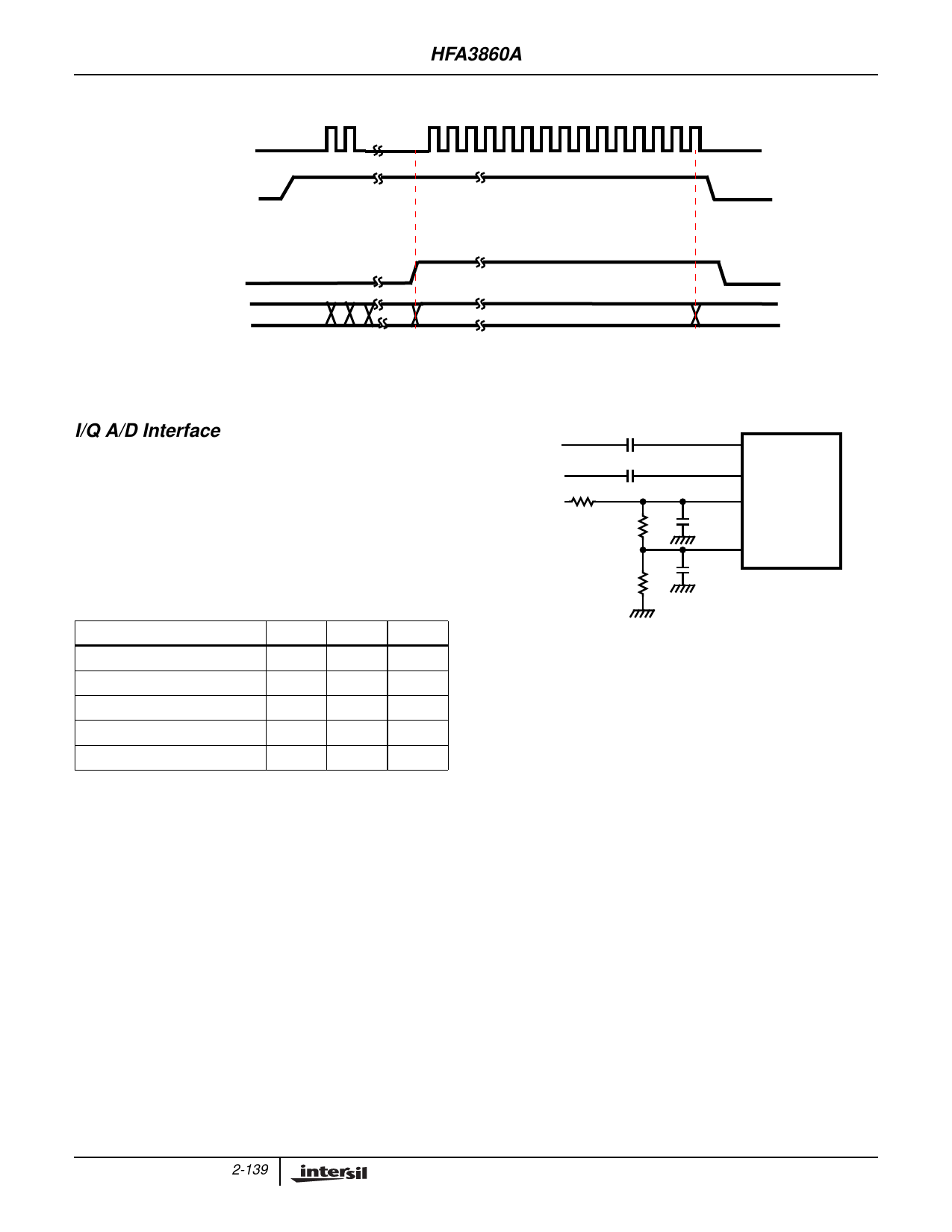
I/Q A/D Interface
The PRISM baseband processor chip (HFA3860A) includes
two 3-bit Analog to Digital converters (A/Ds) that sample the
analog input from the IF down converter. The I/Q A/D clock,
samples at twice the chip rate. The nominal sampling rate is
22MHz.
The interface specifications for the I and Q A/Ds are listed in
Table 2.
TABLE 2. I, Q, A/D SPECIFICATIONS
PARAMETER
MIN
TYP
Full Scale Input Voltage (VP-P)
Input Bandwidth (-0.5dB)
0.25
0.50
-
20MHz
Input Capacitance (pF)
-
5
Input Impedance (DC)
5kΩ
-
FS (Sampling Frequency)
-
22MHz
MAX
1.0
-
-
-
-
The voltages applied to pin 16, VREFP and pin 17, VREFN
set the references for the internal I and Q A/D converters. In
addition, VREFP is also used to set the RSSI A/D converter
reference. For a nominal I/Q input of 500mVP-P, the
suggested VREFP voltage is 1.75V, and the suggested
VREFN is 0.86V. VREFN should never be less than 0.25V.
Figure 6 illustrates the suggested interface configuration for
the A/Ds and the reference circuits.
Since these A/Ds are intended to sample AC voltages, their
inputs are biased internally and they should be capacitively
coupled. The HPF corner frequency in the baseband receive
path should be less than 1kHz.
.
I
Q
3.9K
2V
0.15µF
0.15µF
8.2K
9.1K
IIN
0.01µF
QIN
VREFP
0.01µF
VREFN
HFA3860A
FIGURE 6. INTERFACES
The A/D section includes a compensation (calibration) circuit
that automatically adjusts for temperature and component
variations of the RF and IF strips. The variations in gain of
limiters, AGC circuits, filters etc. can be compensated for up
to ±4dB. Without the compensation circuit, the A/Ds could
see a loss of up to 1.5 bits of the 3 bits of quantization. The
A/D calibration circuit adjusts the A/D reference voltages to
maintain optimum quantization of the IF input over this
variation range. It works on the principle of setting the
reference to insure that the signal is at full scale (saturation)
a certain percentage of the time. Note that this is not an
AGC and it will compensate only for slow variations in signal
levels (several seconds).
The procedure for setting the A/D references to
accommodate various input signal voltage levels is to set the
reference voltages so that the A/D calibration circuit is
operating at half scale with the nominal input. This leaves
the maximum amount of adjustment room for circuit
tolerances.
2-139
Share Link: 