W216 データシートの表示(PDF) - Cypress Semiconductor
部品番号
コンポーネント説明
一致するリスト
W216 Datasheet PDF : 14 Pages
| |||
PRELIMINARY
W216
Writing Data Bytes
Each bit in Data Bytes 0–7 controls a particular device function
except for the “reserved” bits which must be written as a logic
0. Bits are written MSB (most significant bit) first, which is bit
7. Table 5 gives the bit formats for registers located in Data
Bytes 0–7.
Table 6 details additional frequency selections that are avail-
able through the serial data interface.
Table 7 details the select functions for Byte 0, bits 1 and 0.
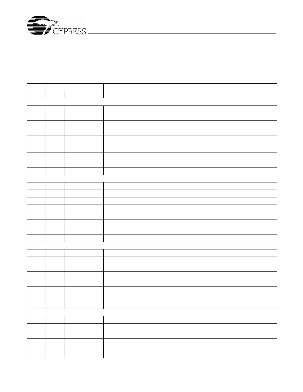
Table 5. Data Bytes 0–7 Serial Configuration Map
Affected Pin
Bit(s) Pin No.
Pin Name
Control Function
Data Byte 0
7
--
--
(Reserved)
6
--
--
SEL2
5
--
--
SEL1
4
--
--
SEL0
Bit Control
0
1
--
--
Refer to Table 6
Refer to Table 6
Refer to Table 6
Default
0
0
0
0
3
--
--
Frequency Table Selection
Frequency Con-
Frequency Con-
0
trolled by FS (3:0) trolled by SEL (3:0)
Table 2
Table 6
2
--
--
SEL3
Refer to Table 6
0
1
-- Spread Spectrum --
OFF
ON
0
0
--
Test Mode
--
Normal
Three-stated
0
Data Byte 1
7
--
6
--
5
--
4
--
3
46
2
49
1
51
0
52
Data Byte 2
7
--
6
8
5
16
4
14
3
13
2
12
1
11
0
9
Data Byte 3
7
--
6
--
5
29
4
30
3 33, 32,
25, 24
--
--
--
--
SDRAM_F
CPU2
CPU1
CPU_F
--
--
--
--
Clock Output Disable
Clock Output Disable
Clock Output Disable
Clock Output Disable
--
PCI_F
PCI5
PCI4
PCI3
PCI2
PCI1
PCI0
(Reserved)
Clock Output Disable
Clock Output Disable
Clock Output Disable
Clock Output Disable
Clock Output Disable
Clock Output Disable
Clock Output Disable
--
--
48MHz
24MHz
SDRAM12:15
(Reserved)
(Reserved)
Clock Output Disable
Clock Output Disable
Clock Output Disable
--
--
0
--
--
0
--
--
0
--
--
0
Low
Active
1
Low
Active
1
Low
Active
1
Low
Active
1
--
--
0
Low
Active
1
Low
Active
1
Low
Active
1
Low
Active
1
Low
Active
1
Low
Active
1
Low
Active
1
--
--
0
--
--
0
Low
Active
1
Low
Active
1
Low
Active
1
6
Share Link: 