V827464K24S データシートの表示(PDF) - Mosel Vitelic Corporation
部品番号
コンポーネント説明
一致するリスト
V827464K24S
Mosel Vitelic Corporation

V827464K24S Datasheet PDF : 14 Pages
| |||
MOSEL VITELIC
V827464K24S
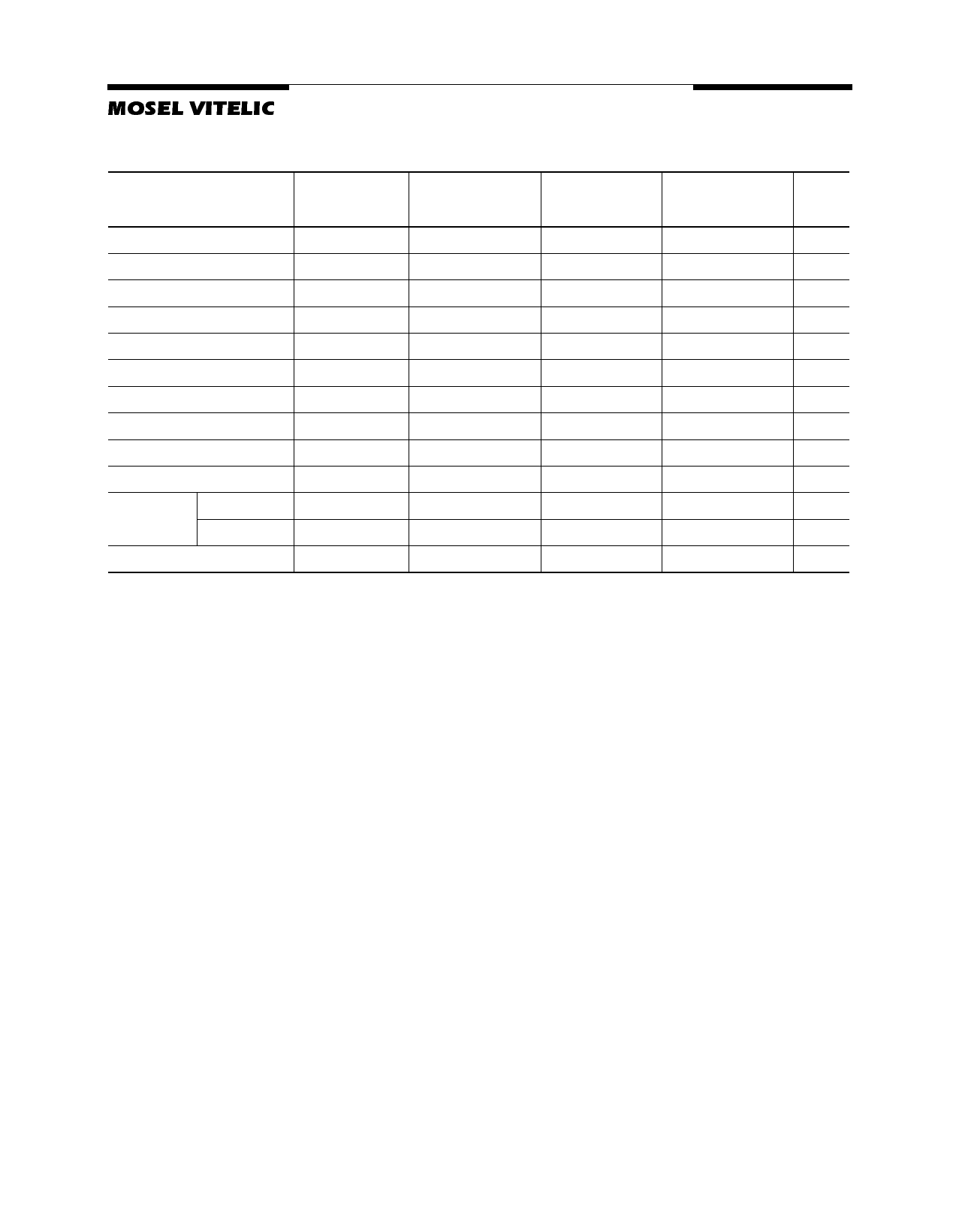
DDR SDRAM IDD SPEC TABLE
Symbol
A1
B0
B1
C0
PC1600@CL=2 PC2100B@CL=2.5 PC2100A@CL=2 PC2100A@CL=2.5 Unit
IDD0
IDD1
IDD2P
IDD2F
IDD2Q
IDD3P
IDD3N
IDD4R
IDD4W
IDD5
IDD6
Normal
Low power
IDD7
680
850
120
440
280
210
360
1150
1180
1600
54
33
1980
870
1100
120
500
340
290
460
1400
1350
1700
54
33
2580
870
1100
120
500
340
290
460
1400
1350
1700
54
33
2580
1060
mA
1280
mA
120
mA
560
mA
380
mA
370
mA
550
mA
1700
mA
1600
mA
1800
mA
54
mA
33
mA
3180
mA
* Module IDD was calculated on the basis of component IDD and can be differently measured according to DQ loading cap.
Detailed test conditions for DDR SDRAM IDD1 & IDD
IDD1 : Operating current: One bank operation
1. Typical Case : Vdd = 2.5V, T=25’ C
2. Worst Case : Vdd = 2.7V, T= 10’ C
3. Only one bank is accessed with tRC(min), Burst Mode, Address and Control inputs on NOP edge are changing once
per clock cycle. lout = 0mA
4. Timing patterns
- DDR200(100Mhz, CL=2) : tCK = 10ns, CL2, BL=4, tRCD = 2*tCK, tRAS = 5*tCK
Read : A0 N R0 N N P0 N A0 N - repeat the same timing with random address changing
*50% of data changing at every burst
- DDR266B(133Mhz, CL=2.5) : tCK = 7.5ns, CL=2.5, BL=4, tRCD = 3*tCK, tRC = 9*tCK, tRAS = 5*tCK
Read : A0 N N R0 N P0 N N N A0 N - repeat the same timing with random address changing
*50% of data changing at every burst
- DDR266A (133Mhz, CL=2) : tCK = 7.5ns, CL=2, BL=4, tRCD = 3*tCK, tRC = 9*tCK, tRAS = 5*tCK
Read : A0 N N R0 N P0 N N N A0 N - repeat the same timing with random address changing
*50% of data changing at every burst
Legend : A=Activate, R=Read, W=Write, P=Precharge, N=NOP
V827464K24S Rev.1.1 September 2002
9
Share Link: