UPD72874 データシートの表示(PDF) - NEC => Renesas Technology
部品番号
コンポーネント説明
一致するリスト
UPD72874 Datasheet PDF : 40 Pages
| |||
µPD72874
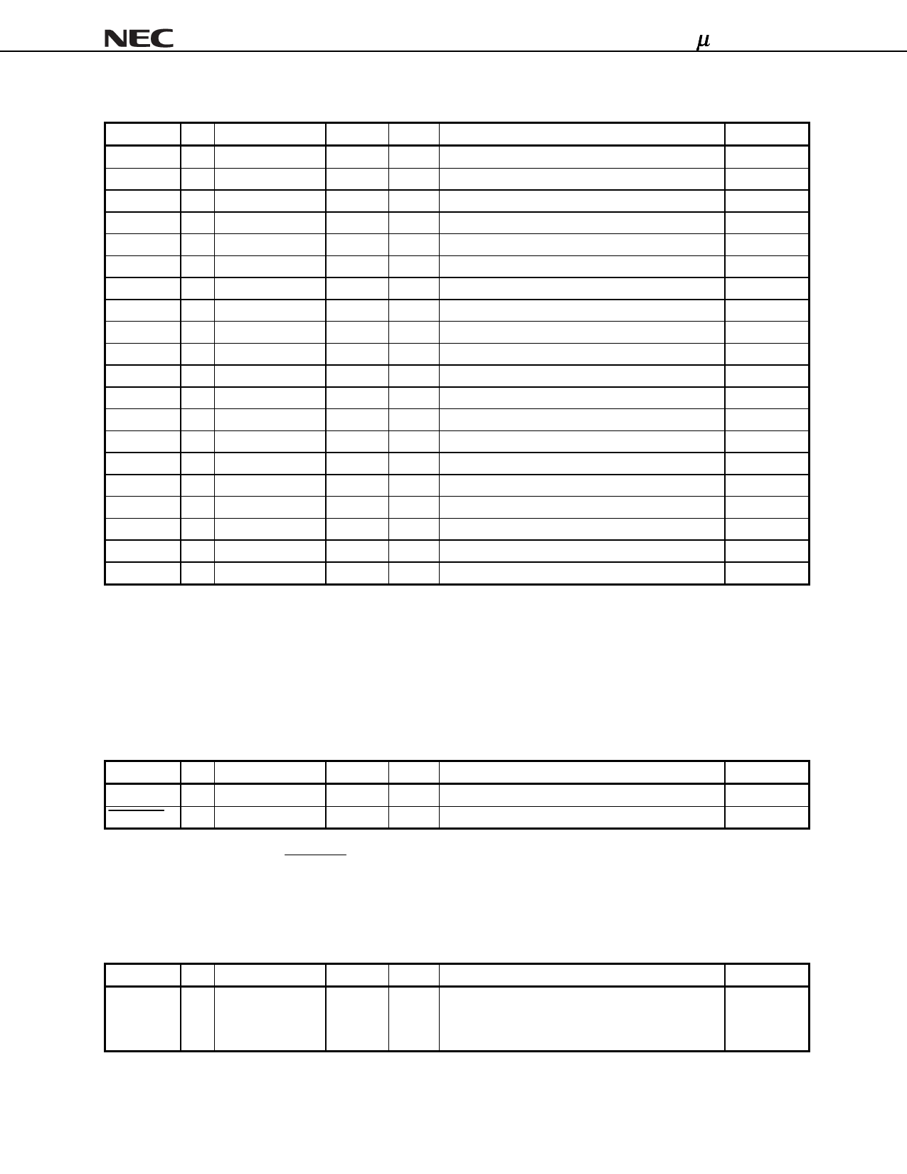
1.2 PHY Signals: (20 pins)
Name
TpA0p
TpA0n
TpB0p
TpB0n
TpA1p
TpA1n
TpB1p
TpB1n
TpA2p
TpA2n
TpB2p
TpB2n
CPS
TpBias0
TpBias1
TpBias2
RI0
RI1
I/O
Pin No.
I/O 101
I/O 100
I/O 99
I/O 98
I/O 105
I/O 104
I/O 103
I/O 102
I/O 110
I/O 109
I/O 108
I/O 107
I 93
O 96
O 97
O 111
- 91
- 92
IOL
Volts(V)
Function
-
- Port-1 Twisted Pair A Positive Input/Output Note 1
-
- Port-1 Twisted Pair A Negative Input/Output Note 1
-
- Port-1 Twisted Pair B Positive Input/Output Note 1
-
- Port-1 Twisted Pair B Negative Input/Output Note 1
-
- Port-2 Twisted Pair A Positive Input/Output Note 1
-
- Port-2 Twisted Pair A Negative Input/Output Note 1
-
- Port-2 Twisted Pair B Positive Input/Output Note 1
-
- Port-2 Twisted Pair B Negative Input/Output Note 1
-
- Port-3 Twisted Pair A Positive Input/Output Note 1
-
- Port-3 Twisted Pair A Negative Input/Output Note 1
-
- Port-3 Twisted Pair B Positive Input/Output Note 1
-
- Port-3 Twisted Pair B Negative Input/Output Note 1
-
-
Cable Power Status Input Note2
-
- Port-1 Twisted Pair Bias Voltage Output Note 1
-
- Port-2 Twisted Pair Bias Voltage Output Note 1
-
- Port-3 Twisted Pair Bias Voltage Output Note 1
-
- Resistor0 for Reference Current Setting Note 3
-
- Resistor1 for Reference Current Setting Note 3
XI
I 87
-
- X’tal XI
XO
O 88
-
- X’tal XO
Notes 1. If unused port, please refer to 4.1.4 Unused Ports.
2. Please refer to 4.1.3 CPS.
3. Please refer to 4.5 RI0, RI1.
Block *
PHY Analog
PHY Analog
PHY Analog
PHY Analog
PHY Analog
PHY Analog
PHY Analog
PHY Analog
PHY Analog
PHY Analog
PHY Analog
PHY Analog
PHY Digital
PHY Analog
PHY Analog
PHY Analog
PHY Analog
PHY Analog
PHY Analog
PHY Analog
Remark *: If the PHY Digital pin is pulled up, it should be connected to P_DVDD.
If the PHY Analog pin is pulled up, it should be connected to P_AVDD.
1.3 PHY Control Signals: (4 pins)
Name
I/O
Pin No.
IOL
PC0 to PC2 I 70 to 72
-
P_RESET
I 81
-
Notes 1. Please refer to 4.3 PC0 to PC2.
2. Please refer to 4.4 P_RESET.
Volts(V)
Function
3.3 Power Class Input Note 1
-
PHY Power on Reset Input Note 2
Remark *: If the PHY Digital pin is pulled up, it should be connected to P_DVDD.
Block *
PHY Digital
PHY Digital
1.4 PCI/Cardbus Select Signal: (1 pin)
Name
I/O
Pin No.
IOL
Volts(V)
Function
CARD_ON I 119
-
3.3 PCI/CardBus Select
1:Cardbus mode
0:PCI bus mode
Remark *: If the Link pin is pulled up, it should be connected to L_VDD.
Block *
Link
10
Preliminary Data Sheet S15306EJ2V0DS
Share Link: 