UPD72862 データシートの表示(PDF) - NEC => Renesas Technology
部品番号
コンポーネント説明
一致するリスト
UPD72862 Datasheet PDF : 36 Pages
| |||
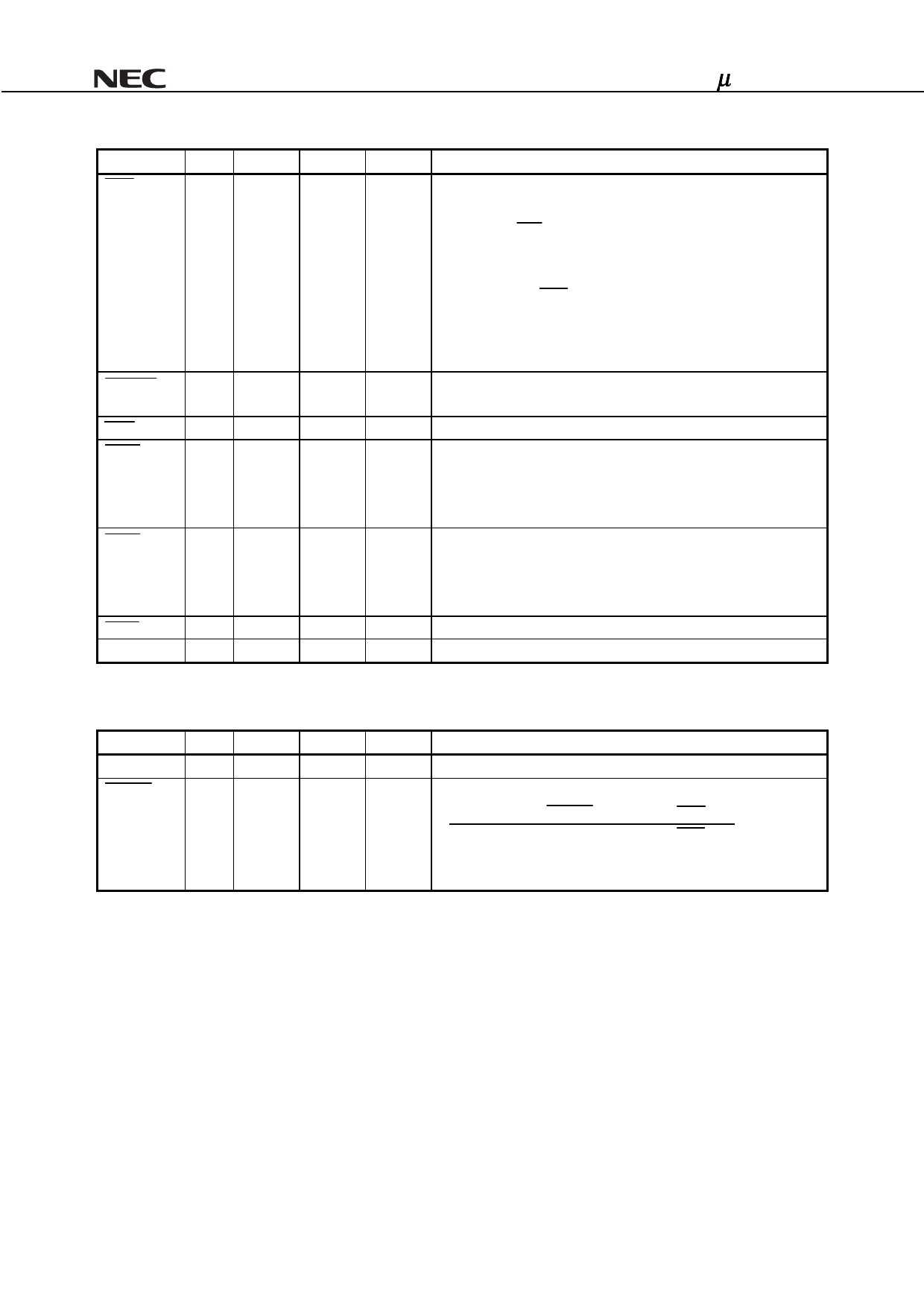
µPD72862
Name
PME
5
I/O Pin No.
IOL
Volts(V)
Function
O 79
PCI/Cardbus 5/3.3 PME Output for power management enable.
(2/2)
Caution The PME pin is not an N-channel open drain structure pin.
Therefore, when using S3, S4, S5 state in ACPI, a
circuit that can separate between the power supply
and the PME pin externally is needed.
CLKRUN
INTA
PERR
I/O 78
O 80
I/O 16
SERR
O 17
PRST
PCLK
I 81
I 82
PCI/Cardbus
PCI/Cardbus
PCI/Cardbus
PCI/Cardbus
-
-
5/3.3
5/3.3
5/3.3
5/3.3
5/3.3
5/3.3
ACPI: Advanced Configuration and Power Interface.
Please refer to ACPI Specification.
PCICLK Running as input, to determine the status of PCLK; as
output, to request starting or speeding up clock.
Interrupt the PCI interrupt request A.
Parity Error is used for reporting data parity errors during all PCI
transactions, except a Special Cycle. It is an output when AD0-
AD31 and PAR are both inputs. It is an input when AD0-AD31 and
PAR are both outputs.
System Error is used for reporting address parity errors, data parity
errors during the Special Cycle, or any other system error where the
effect can be catastrophic. When reporting address parity errors, it
is an output.
Reset PCI reset
PCI Clock 33 MHz system bus clock.
1.2 PCI/Cardbus Select Signals: (2 pins)
Name
I/O Pin No.
IOL
Volts(V)
Function
CARD_ON
I 54
-
3.3
PCI/Card Select (1:Cardbus, 0:PCI bus)
CIS_ON
I 45
-
3.3
CIS Register ON
CARD_ON CIS_ON CIS
PME
0
1
off
PME
0
0
on CSTSCHG
1
X
on CSTSCHG
Data Sheet S14265EJ2V0DS00
9
Share Link: 