UPD72852 データシートの表示(PDF) - NEC => Renesas Technology
部品番号
コンポーネント説明
一致するリスト
UPD72852 Datasheet PDF : 48 Pages
| |||
µPD72852
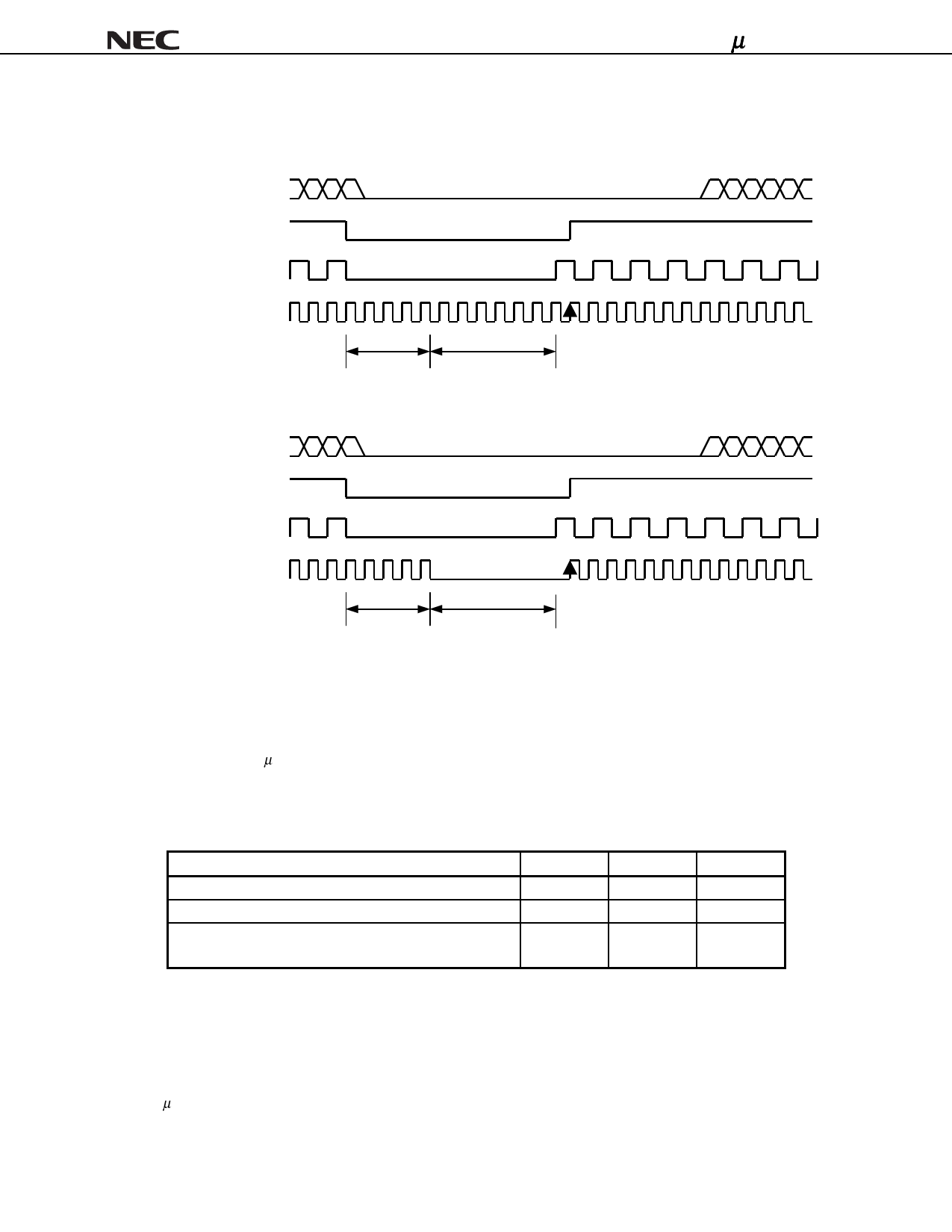
Figure 4-2. PHY/Link Interface Reset and Disable
D, CTL, LREQ
LPS
LPS
(with isolation barrier)
SCLK
(a) Reset
D, CTL, LREQ
LPS
LPS
(with isolation barrier)
SCLK
tLPS_RESET
tRESTORE
(b) Disable
tLPS_DISABLE
tRESTORE
4.2 Link-on Indication
When the power supply of Link is off (LPS is Low and the internal PHY register Link_active bit is 0), the pin LKON
outputs a clock of 6.144 MHz according to the following conditions:
• Link-on packet is received.
• When any bit of the µPD72852 PHY register’s loop, Pwr_fail, Timeout or Port_event becomes 1, and either LPS
or the Link_active bit is 0.
Table 4-2. Link-on Timing
Parameter
Frequency
Duty Cycle
Propagation delay before the Link becomes active (LPS is
asserted and the Link_active bit in the PHY register is 1).
MIN.
4
40
MAX.
8
60
500
Unit
MHz
%
ns
• If LPS or the Link_active bit is 0, the Link is considered inactive.
When the Link is inactive and any of Loop, Pwr_fail, Timeout, Port_event becomes 1, then Link-on is asserted
High.
• When the Link is active (both LPS and Link_active become 1) and Loop, Pwr_fail, Timeout and Port_event
become 1, Status transfer is sent on the PHY/Link interface.
• The µPD72852 activates the PHY/Link interface when LPS is 1, regardless of the value of the Link active bit.
Data Sheet S14920EJ3V0DS
21
Share Link: 