UPD161660 データシートの表示(PDF) - NEC => Renesas Technology
部品番号
コンポーネント説明
一致するリスト
UPD161660 Datasheet PDF : 15 Pages
| |||
µPD161660
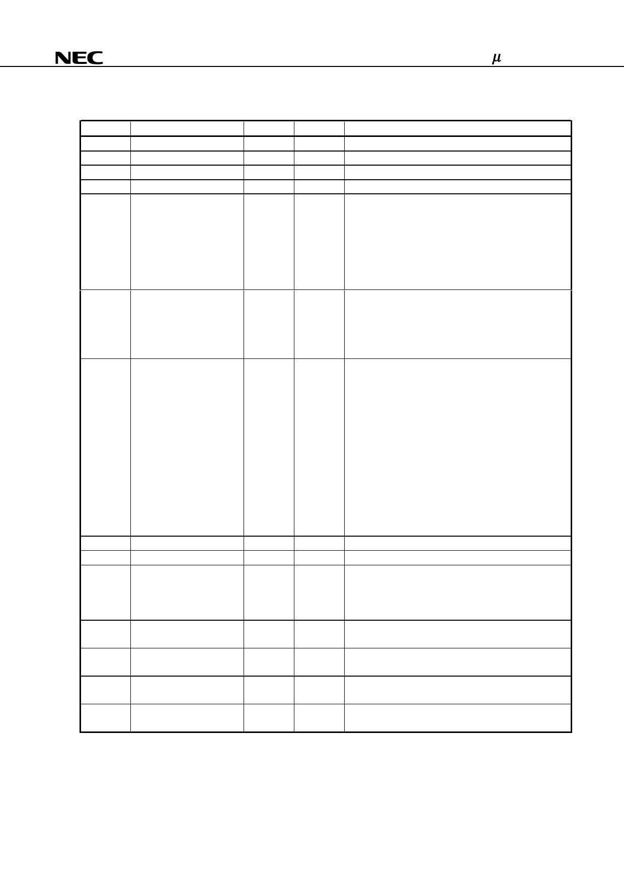
3. PIN FUNCTIONS
Symbol
VDC
VCC1
VSS
DVSS
VDD1
Pin Name
Power supply
Power supply
Ground
Ground
DC/DC converter output
Pad No.
7
42
40
49
15
VDD2
DC/DC converter output
16
VO
Rectangle signal output for
19
negative boost
VT
Regulator output
13
VS
Regulator output
10
VREF
Reference voltage
12
input/output
DCON
DC/DC converter control
64
RGONP Regulator control
65
EXRVT
VT regulating resistor
63
selection
EXRVS
VS regulating resistor
62
selection
(1/2)
I/O
Description
–
Power supply for DC/DC converter.
–
Power supply for logic circuit.
–
Ground.
–
Ground (for control pin pull-down)
–
Boost voltage of DC/DC converter (x4, x5, x6 or x7).
The capacitors required for each boost level are shown
below.
• x4 boost: C1, C2, C6 (C3, C4, and C5 are not required)
• x5 boost: C1, C2, C3, C6 (C4, and C5 are not required)
• x6 boost: C1, C2, C3, C4, C6 (C5 is not required)
• x7 boost: C1, C2, C3, C4, C5, C6
–
Boost voltage of DC/DC converter (x2 or x3). The boost
steps for VDD2 is selected by VCD2 pin. The capacitors
required for each boost level are shown below.
• x2 boost: C1
• x3 boost: C1, C2,
–
Rectangle signal output for negative boost. The VO voltage
range is selected by VCE pin. The capacitors required for
each boost level are shown below.
<VCE = L>
• x3 boost: C1, C2
• x4 boost: C1, C2, C3
• x5 boost: C1, C2, C3, C4
• x6 boost: C1, C2, C3, C4, C5
<VCE = H>
• x4 boost: C1, C2, C6
• x5 boost: C1, C2, C3, C6
• x6 boost: C1, C2, C3, C4, C6
• x7 boost: C1, C2, C3, C4, C5, C6
–
15 V/12.5 V regulator output for gate driver.
–
5 V/4 V regulator output for source driver.
I/O
The gate driver includes reference voltage for VB regulator.
When VREFSEL = H, external reference voltage can be
input. Reference voltage input/output pin of VT, VS
regulator.
I
DC/DC converter ON/OFF control. Connect to DCON pin
of source driver.
I
Regulator ON/OFF control. Connect to RGONP pin of
source driver.
I
To select internal/external resistor for VT regulator.
I
To select internal/external resistor for VS regulator.
Data Sheet S14799E1V0DS
5
Share Link: 