UPD161660 データシートの表示(PDF) - NEC => Renesas Technology
部品番号
コンポーネント説明
一致するリスト
UPD161660 Datasheet PDF : 15 Pages
| |||
µPD161660
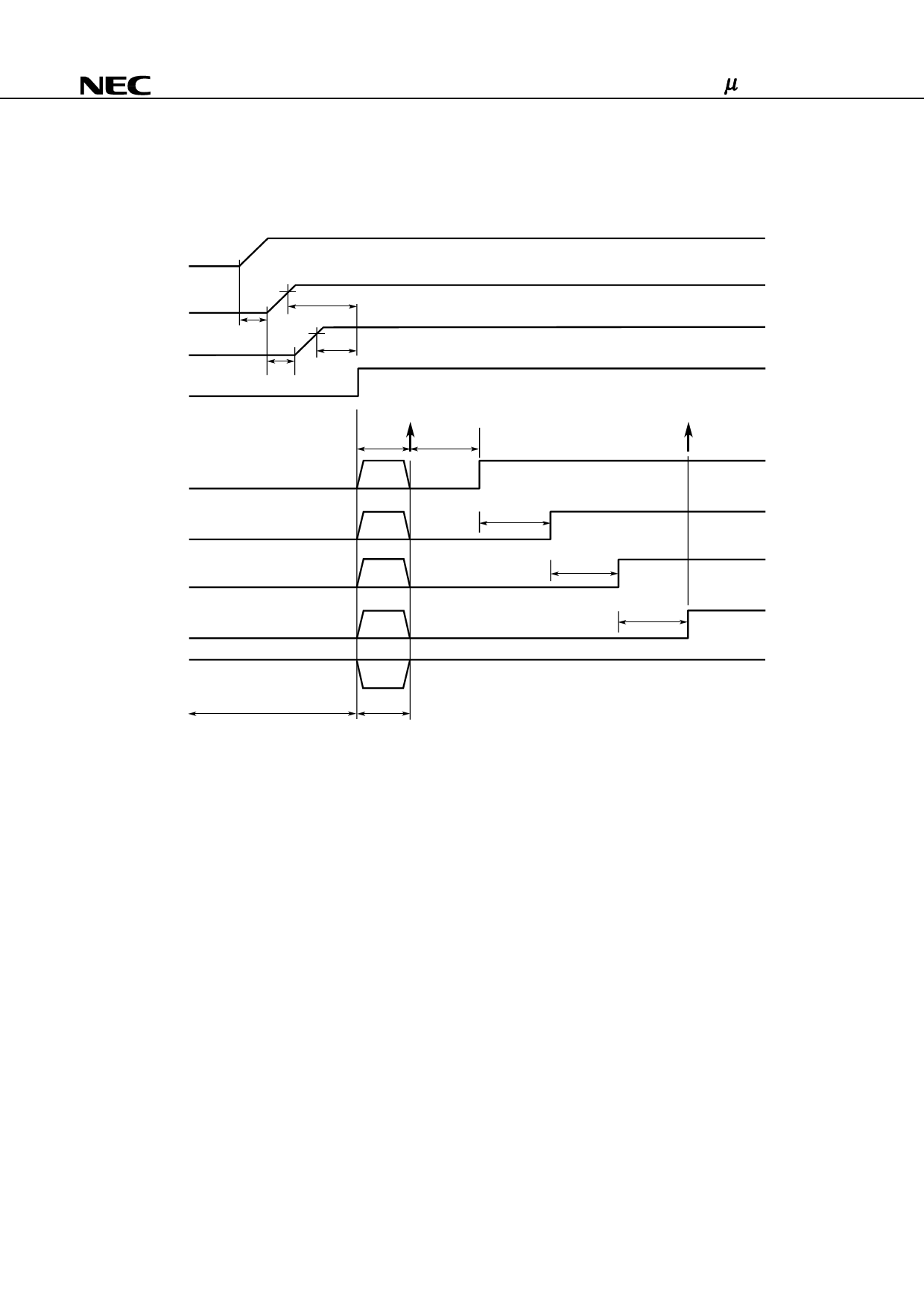
5. POWER ON/OFF SEQUENCE
5.1 Power ON sequence
VDC
VCC1
VCC2
/RESET
DCON
2.5 V
tVR1
0 ns
1.7 V
tVR2
0 ns
RESET
command
100 ns <
0 ns
RGONP
RGONG
OE1
OE2
A
B
DISP ON
command
tDDRP
tRPRG
tRGOE1
tVR1, tVR2 = 100 ns MIN.
Remarks 1. /xxx indicates active low signal.
2. OE1, OE2, /RESET, RGONG, RGONP, VCC2 are signals from source driver.
x All three power supplies, VDC, VCC1, and VCC2, can be on at the same time.
y The pins are fixed to the following levels by the source driver during the period of /RESET = L (A period).
Note that the gate output is fixed to the VB level, and the DC/DC converter and the regulators are off.
DCON, RGONG, RGONP, OE1: L (low level)
OE2: H (high level)
z The /RESET pin can be made high at the end of both tVR1, which starts from the rising edge of VCC1, and tVR2, which
starts from the rising edge of VCC2.
{ The wait time between when the /RESET signal rises and when the RESET command is acknowledged must be at
least 100 ns.
| The logical status of the DCON, RGONG, RGONP, OE1, and OE2 pins in the period between when the /RESET
signal rises and when the RESET command (↑part) is acknowledged (B period) is undefined. Be aware, therefore,
10
Data Sheet S14799EJ1V0DS
Share Link: 