UPD161620 データシートの表示(PDF) - NEC => Renesas Technology
部品番号
コンポーネント説明
一致するリスト
UPD161620 Datasheet PDF : 71 Pages
| |||
µ PD161620
3. PIN FUNCTIONS
3.1 Power Supply System Pins
Symbol
VCC1
VCC2
VS
VSS
5 V0 to V15
VRH
VRL1, VRL2
5 DVCC1
5 DVSS
Pin Name
Pad No.
Logic power supply pin 490 to 492
I/O power supply pin 509 to 511
Driver power supply pin 484 to 486
Ground pin
Power supply for
γ-curve correction
487 to 489
476 to 461
477, 460, 459
Mode setting pull-up 448,480,531,
power-supply pin
535,539,544
Mode setting pull-down 453,481,529,
power-supply pin
533,537,542,
546
I/O
Function
- Power supply pin for logic circuit
- Power supply pin for I/O buffer
- Power supply pin for driver circuit
- Ground pin for logic and driver circuits
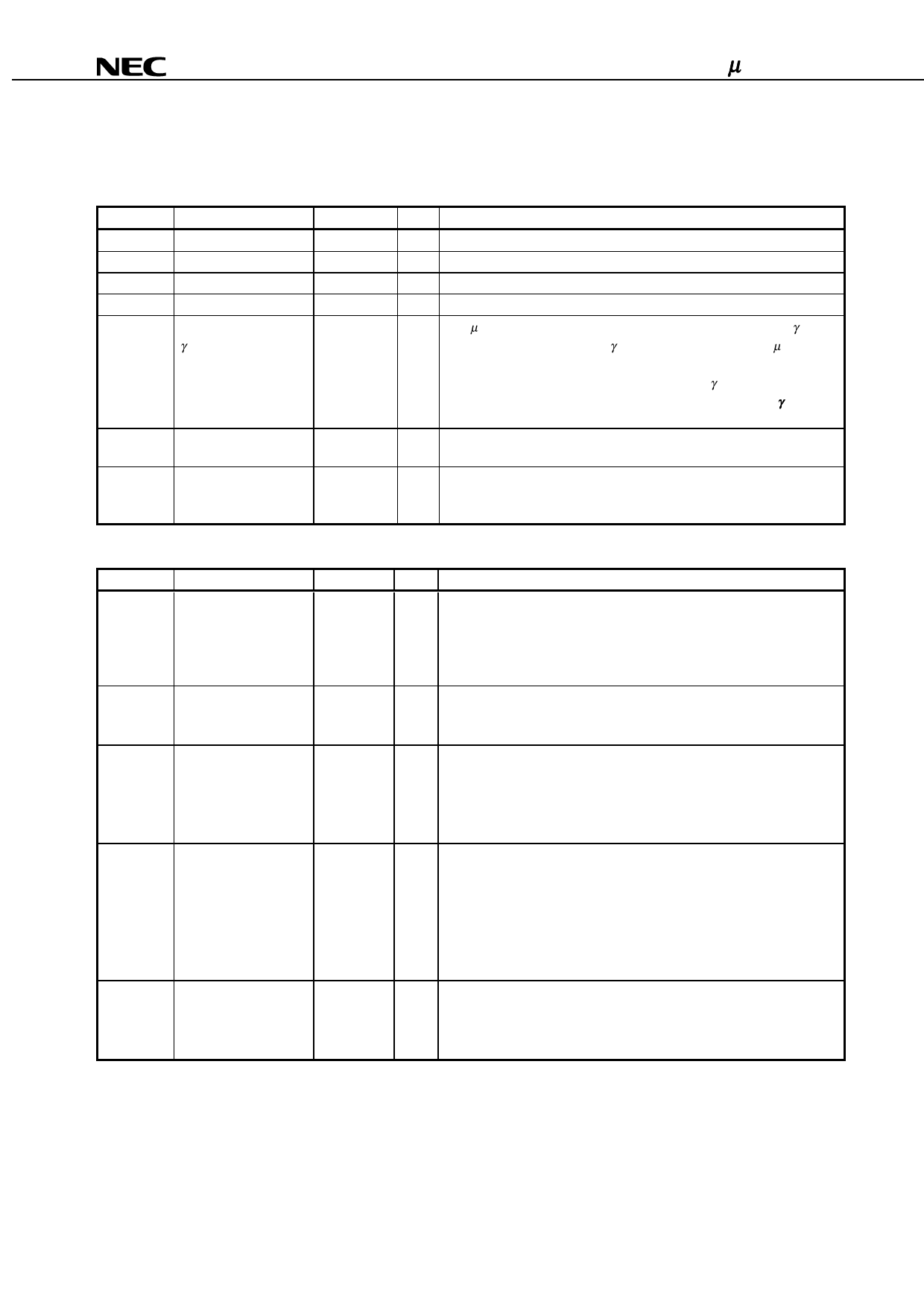
- The µ PD161620 includes power supplies and resistors for the γ-curve,
so if the characteristics of the γ-curve and LCD panel in the µ PD161620
match, leave V0 to V15, VRH, VRL1, VRL2 open.
If some kind of correction is required, adjust the γ-curve by connecting
resistors between the V0 to V15, VRH, VRL1, VRL2 pins (see 5.9 γ-Curve
Correction Power Supply Circuit for Cases of Unbalanced Driving).
- Pull-up power-supply pin for mode setting
- Pull-down power-supply pin for mode setting
3.2 Logic System Pins
Symbol
Pin Name
Pad No.
PSX0, PSX1 CPU interface selection 534, 532
/CS1,
Chip select
525,
CS2
512
/RD
Read (enable)
514
(E)
5 /WR
Write(read/write)
515
(R, /W)
C86
Select interface
536
(1/3)
I/O
Function
Input These pins are used to select the CPU interface mode.
PSX0 = H: 8-bit parallel interface
PSX0 = L: 4-bit parallel interface
PSX1 = H: Parallel interface
PSX1 = L: Serial interface
Input This pin is used for chip select signals. When /CS1 = L (CS2 = H),
the chip is active and can perform data input/output operations including
command and data I/O.
Input When i80 series parallel data transfer (/RD) has been selected, the
signal at this pin is used to enable read operations. Data is output to the
data bus only when this pin is low.
When M68 series parallel data transfer (E) has been selected, the signal
at this pin is used to enable read/write operations.
Input When i80 series parallel data transfer (/WR) has been selected, the
signal at this pin is used to enable write operations. Data is written at
the rising edge of this signal.
When M68 series parallel data transfer (R, /W) and serial data has been
selected, this pin is used to determine the direction of data transfer.
L: Write
H: Read
Input This pin is used to switch between interface modes (i80 series CPU or
M68 series CPU).
L: Selects i80 series CPU mode
H: Selects M68 series CPU mode
8
Preliminary Product Information S14797EJ3V7PM
Share Link: 