S8208(2004) データシートの表示(PDF) - Toshiba
部品番号
コンポーネント説明
一致するリスト
S8208 Datasheet PDF : 7 Pages
| |||
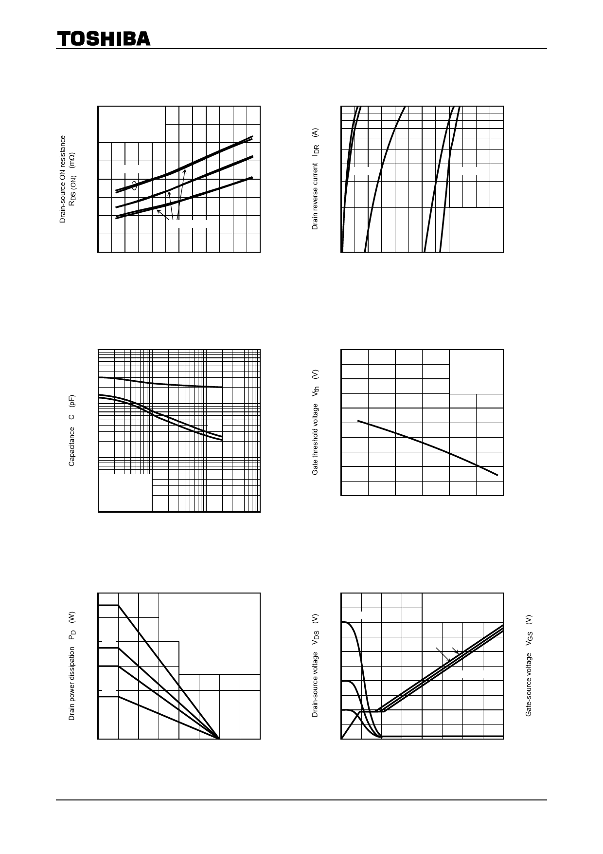
RDS (ON) – Ta
40
Common source
35
Pulse test
30
25
VGS = 2 V
2.5
20
4
15
10
ID = 1.5, 3, 6 A
5
0
−80
−40
0
40
80
120
160
Ambient temperature Ta (°C)
TPCS8208
IDR – VDS
10
10, 5, 3 1
3
0
VGS = −1 V
Common source
Ta = 25°C
Pulse test
1
0
−0.2 −0.4 −0.6 −0.8 −1.0 −1.2
Drain-source voltage VDS (V)
10000
Capacitance – VDS
Ciss
1000
Coss
Crss
100
Common source
Ta = 25°C
VGS = 0 V
f = 1 MHz
10
0.1
1
10
100
Drain-source voltage VDS (V)
2.0
1.8
1.6
1.4
1.2
1.0
0.8
0.6
0.4
0.2
0
−80
Vth – Ta
Common source
VDS = 10 V
ID = 200 µA
Pulse test
−40
0
40
80
120
160
Ambient temperature Ta (°C)
1.2
(1)
1
0.8 (2)
(3)
0.6
0.4 (4)
0.2
PD – Ta
Device mounted on a glass-epoxy
board (a)
(Note 2a)
(1) Single-device operation (Note 3a)
(2) Single-device value at dual
operation
(Note 3b)
Device mounted on a glass-epoxy
board (b)
(Note 2b)
(3) Single-device operation
(Note 3a)
(4) Single-device value at dual
operation
(Note 3b)
t = 10 s
0
0
50
100
150
200
Ambient temperature Ta (°C)
Dynamic input/output characteristics
20
10
Common source
VDD = 16 V
16
ID = 6 A
Ta = 25°C, Pulse test
8
12
8
8
VDS
4
4
84
6
VDD = 16 V
4
VGS
2
0
0
0
8
16
24
32
Total gate charge Qg (nC)
5
2004-07-06
Share Link: 