PI6C110EV データシートの表示(PDF) - Pericom Semiconductor
部品番号
コンポーネント説明
一致するリスト
PI6C110EV Datasheet PDF : 15 Pages
| |||
PI6C110E 111222333444555666777888999000111222333444555666777888999000111222333444555666777888999000111222111222333444555666777888999000111222333444555666777888999000111222333444555666777888999000111222111222333444555666777888999000111222333444555666777888999000111222333444555666777888999000111222111222333444555666777888999000111222333444555666777888999000111222333444555666777888999000111222111222333444555666777888999000111222
Clock Solution for 133 MHz
Celeron/Pentium II/III Processors
Features
3 of 2.5V 66/100/133 MHz CPU (CPU[0-2])
2 of 2.5V 33 MHz APIC (APIC[0-1])
9 of 3.3V 100/133 MHz SDRAM (SDRAM[0-7], DCLK)
8 of 3.3V 33 MHz PCI (PCI[0-7])
2 of 3.3V 66 MHz (3V66 [0-1])
2 of 3.3V 48 MHz (48MHz [0-1])
1 of 3.3V 14.3 MHz (REF)
Selectable CPU and SDRAM clocks (on power up only)
Power down function using PWR_DWN#
Spread Spectrum Enable/Disable by I2C
I2C interface to turn off unused clocks
56 pin SSOP package (V)
Description
Pericom PI6C110E integrates a dual PLL clock generator, SDRAM
buffer and I2C interface. The clock generator section comprised
of an oscillator, 2 low jitter phased locked loop, skew control, and
power down logic. The SDRAM buffers are high speed and low
skew to handle data transfers in excess of 133 MHz.
When Spread Spectrum mode is enabled, all clock outputs are
modulated except for REF and 48 MHz[0-1] outputs. These clocks
are down spread linearly (triangular modulation) by +0%, 0.6%.
To minimize power consumption and EMI radiation some unused
outputs can be turned off. Two wire I2C interface is used to enable/
disable Spread Spectrum mode, and to turned off PCI clocks, CPU
clocks, and 48 MHz clocks.
For low power sleep mode, the entire device can be placed to power
down mode. Driving the PWR_DWN# to low state disables the
entire chip. In this state the crystal oscillator, and both PLLs are
turned off. Furthermore, all outputs are deactivated to low state, all
inputs are inactive except for PWR_DWN#.
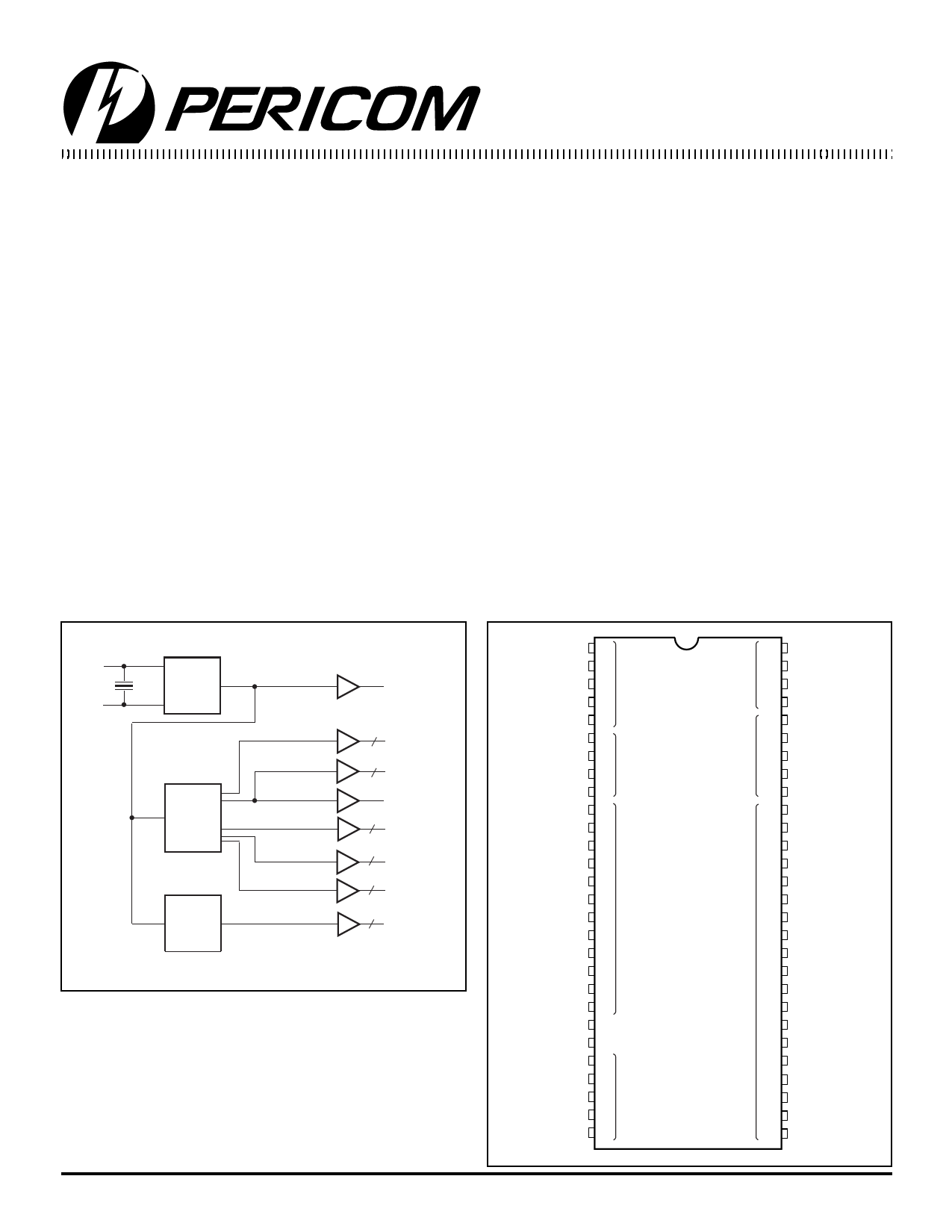
Block Diagram
Pin Configuration
XIN
XOUT
REF
OSC
PLL1
PLL2
All trademarks are of their respective companies.
REF
3
CPU 0-2
8
SDRAM 0-7
DCLK
8
PCI 0-7
2
APIC 0-1
2
3V66 0-1
2
48 MHz 0-1
REF/SEL2
VDD3.3
XTAL_IN
XTAL_OUT
VSS3.3
VSS3.3
3V66 0
3V66 1
VDD3.3
VDD3.3
PCI 0
PCI 1
PCI 2
VSS3.3
PCI 3
PCI 4
VSS3.3
PCI 5
PCI 6
PCI 7
VDD3.3
VDDA
VSSA
VSS3.3
48MHz0
48MHz1
VDD3.3
SEL0
1
2
3 3.3V
4
5
6
7
8
3.3V
9
10
11
12
13
14
15
16
3.3V
17
18
19
20
21
22
23
24
25 3.3V
26
27
28
56-Pin
(VV56)
56
2.5V
55
54
53
52
51
2.5V 50
49
48
47
46
45
44
43
42
41
40
39
3.3V 38
37
36
35
34
33
32
31
30
29
VSS2.5
APIC0
APIC1
VDD2.5
CPU 0
VDD2.5
CPU 1
CPU 2
VSS2.5
VSS3.3
SDRAM0
SDRAM1
VDD3.3
SDRAM2
SDRAM3
VSS3.3
SDRAM4
SDRAM5
VDD3.3
SDRAM6
SDRAM7
VSS3.3
DCLK
VDD3.3
PWR_DWN#
SCLK
SDATA
SEL1
1
PS8410
08/11/99
Share Link: 