TC58DVM92A1FTI0 データシートの表示(PDF) - Toshiba
部品番号
コンポーネント説明
一致するリスト
TC58DVM92A1FTI0 Datasheet PDF : 44 Pages
| |||
TC58DVM92A1FTI0
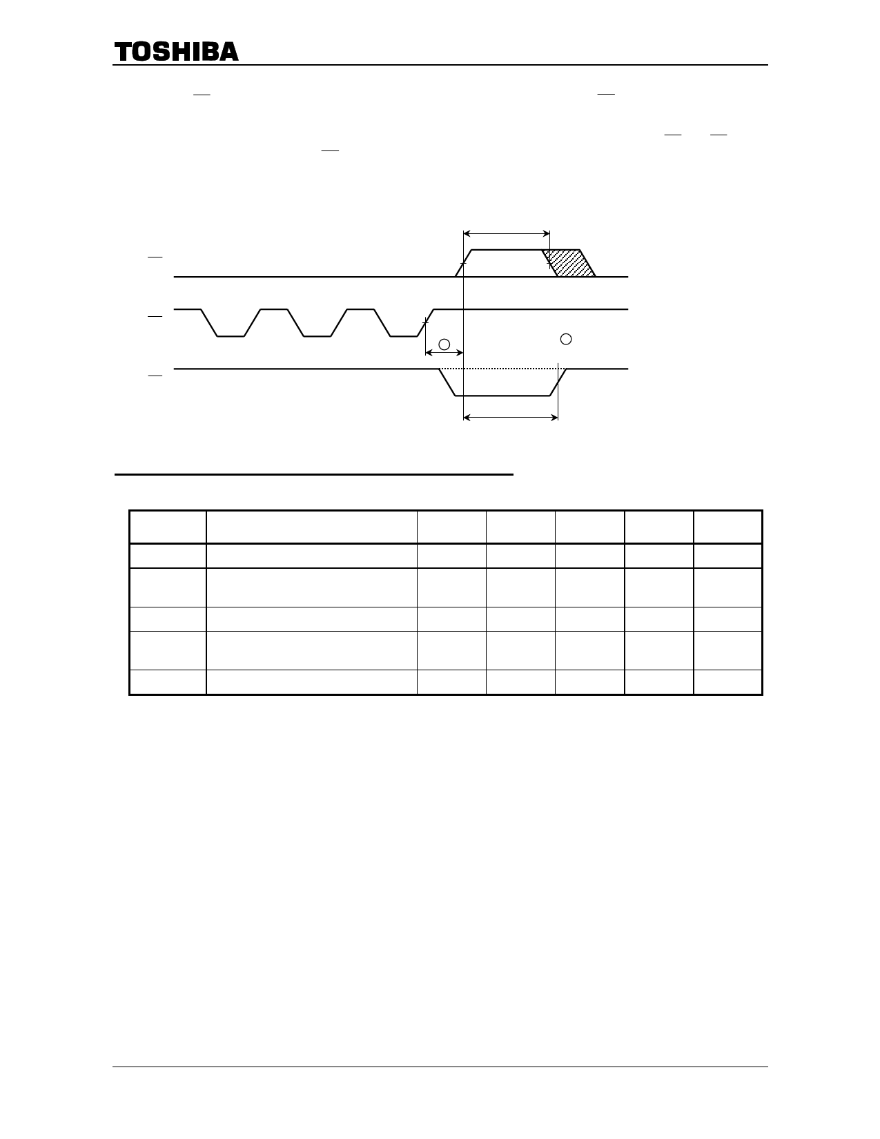
Note: (1) CE High to Ready time depends on the pull-up resistor tied to the RY/BY pin.
(Refer to Application Note (9) toward the end of this document.)
(2) Sequential Read is terminated when tCEH is greater than or equal to 100 ns. If the RE to CE delay
is less than 30 ns, RY/BY signal stays Ready.
tCEH t 100 ns
*
*: VIH or VIL
CE
RE
525
526
527 A
A : 0 to 30 ns oBusy signal is not output.
RY/BY
Busy
tCRY
PROGRAMMING AND ERASING CHARACTERISTICS
(Ta - 40° to 85°C, VCC 2.7 V to 3.6 V)
SYMBOL
PARAMETER
MIN
tPROG
Programming Time
Dummy Busy Time for Multi Block
tDBSY
Programming
tMBPBSY
Multi Block Program Busy Time
N
Number of Programming Cycles on Same
Page
tBERASE
Block Erasing Time
(1): Refer to Application Note (12) toward the end of this document.
TYP.
200
2
200
2
MAX
1000
10
1000
3
10
UNIT
Ps
Ps
Ps
ms
NOTES
(1)
2003-07-11 5/44
Share Link: 