IMISM561BZ データシートの表示(PDF) - Cypress Semiconductor
部品番号
コンポーネント説明
一致するリスト
IMISM561BZ Datasheet PDF : 8 Pages
| |||
Device
SM561
Example:
Device
Fin
Range
Then;
Cdiv
2332
(All Ranges)
= SM561
= 65 MHz
= S1 = 1, S0 = 0
Modulation Rate = Fmod = 65 MHz/2332 = 27.9 kHz.
SM561
Modulation Profile
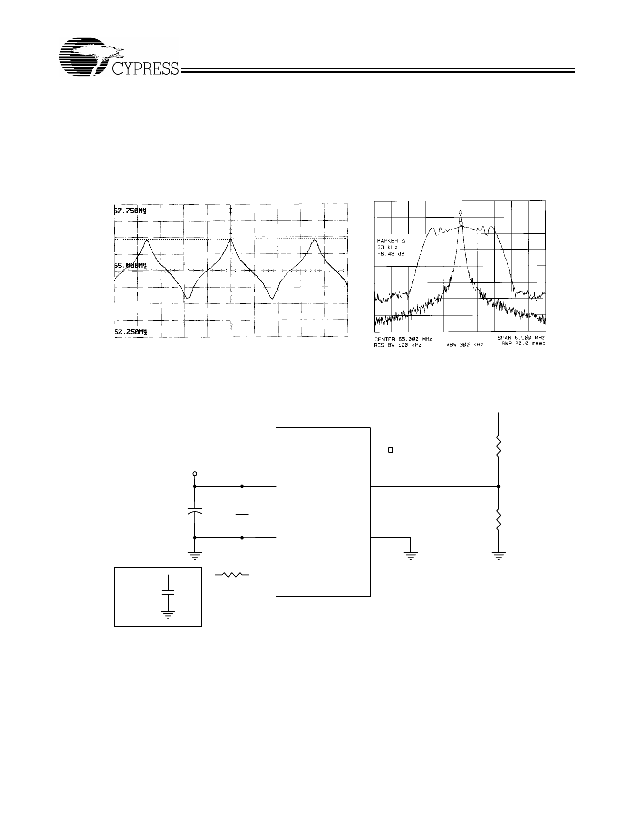
Spectrum Analyzer
Figure 2. SSCG Clock, SM561, Fin = 65 MHz
SM560 Application Schematic
VDD
65 MHz Reference Clock
R2
1 Xin/CLK
Xout 8
20 K
VDD
2 VDD
S0 7
C5
C6
R4
22 uF.
0.1 uF
20 K
3
GND
6
S1
Application Load
R5
4 SSCLK
SSCC 5
VDD
22
SM561
Figure 3. Application Schematic
The schematic in Figure 3 demonstrates how SM561 is
configured in a typical application. This application uses a
65-MHz reference clock connected to pin 1. Because an
external reference clock is used, pin 8 (Xout) is left uncon-
nected.
Figure 3 also demonstrates how to properly use the Tri-level
Logic employed in the SM561. Note that resistors R2 and R4
create a voltage divider that places VDD/2 on pin 7 to satisfy
the voltage requirement for an “M” state.
With this configuration, the SM561 will produce an SSCG
clock that is at a center frequency of 65 MHz. Referring to
Table 1, range “0, M” at 65 MHz will generate a modulation
profile that has a 1.7% peak to peak spread.
Document #: 38-07021 Rev. *C
Page 6 of 8
Share Link: 