IMISM561BZ データシートの表示(PDF) - Cypress Semiconductor
部品番号
コンポーネント説明
一致するリスト
IMISM561BZ Datasheet PDF : 8 Pages
| |||
SM561
.
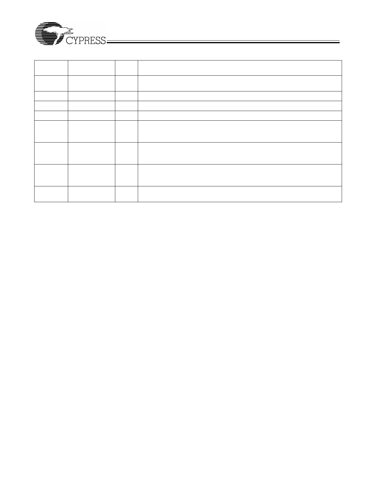
Pin Description
Pin
Number
Pin Name
1
Xin/CLK
2
VDD
3
GND
4
SSCLK
5
SSCC
6
S1
7
S0
8
Xout
Pin
Type
I
P
P
O
I
I
I
O
Pin Description
Clock or Crystal connection input. Refer to Table 1 for input frequency range
selection.
Positive power supply.
Power supply ground.
Modulated clock output.
Spread Spectrum Clock Control (Enable/Disable) function. SSCG function is
enabled when input is high and disabled when input is low. This pin is pulled high
internally.
Tri-level Logic input control pin used to select Frequency and Bandwidth.
Frequency/Bandwidth selection and Tri-level Logic programming. See Figure 1 on
page 3.
Tri-level Logic input control pin used to select Frequency and Bandwidth.
Frequency/Bandwidth selection and Tri-level Logic programming. See Figure 1 on
page 3.
Oscillator output pin connected to crystal. Leave this pin unconnected If an
external clock drives Xin/CLK.
General Description
The Cypress SM561 is a Spread Spectrum Clock Generator
(SSCG) IC used for the purpose of reducing EMI found in
today’s high-speed digital electronic systems.
The SM561 uses a Cypress proprietary phase-locked loop
(PLL) and Spread Spectrum Clock (SSC) technology to
synthesize and frequency modulate the input frequency of the
reference clock. By frequency modulating the clock, the
measured EMI at the fundamental and harmonic frequencies
of Clock (SSCLK) is greatly reduced.
This reduction in radiated energy can significantly reduce the
cost of complying with regulatory requirements and time to
market without degrading the system performance.
The SM561 is a very simple and versatile device to use. The
frequency and spread% range is selected by programming S0
and S1 digital inputs. These inputs use three (3) logic states
including High (H), Low (L), and Middle (M) to select one of the
nine available Frequency Modulation and Spread% ranges.
Refer to Table for programming details.
The SM561 is intended for use with applications with a
reference frequency in the range of 54 to 166 MHz.
A wide range of digitally selectable spread percentages is
made possible by using Tri-level (High, Low, and Middle) logic
at the S0 and S1 digital control inputs.
The output spread (frequency modulation) is symmetrically
centered on the input frequency.
Spread Spectrum Clock Control (SSCC) function enables or
disables the frequency spread and is provided for easy
comparison of system performance during EMI testing.
The SM561 is available in an eight-pin SOIC package with a
0°C-to-70°C operating temperature range.
Refer to the SM560 data sheet for operation at frequencies
from 25 to 108 MHz.
Document #: 38-07021 Rev. *C
Page 2 of 8
Share Link: 