SC4609EVB データシートの表示(PDF) - Semtech Corporation
部品番号
コンポーネント説明
一致するリスト
SC4609EVB Datasheet PDF : 18 Pages
| |||
SC4609
POWER MANAGEMENT
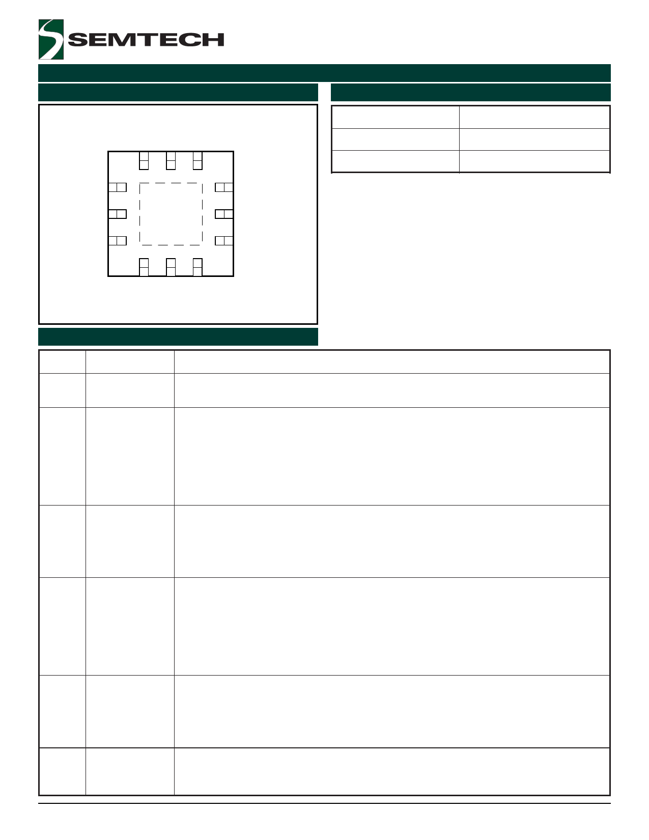
Pin Configuration
TOP VIEW
BST DRVH PHASE
VCC
ISET
COMP
12
11
10
1
9
2
8
3
7
4
5
6
DRVL
PGND
AGND
Ordering Information
Part Number(1)
SC4609MLTRT(2)
SC4609EVB
Device
MLP-12
Evaluation Board
Notes:
(1) Only available in tape and reel packaging. A reel
contains 3000 devices.
(2) Lead free product. This product is fully WEEE and
RoHS compliant.
FSET VSENSE SS
(MLP12, 4x4)
Pin Descriptions
Pin #
1
2
3
4
5
6
Pin Name
VCC
ISET
COMP
FSET
VSENSE
SS
Pin Function
Positive supply rail for the IC. Bypass this pin to GND with a 0.1 to 4.7µF low ESL/ESR
ceramic capacitor.
The ISET pin is used to limit current in the high side MOSFET. The SC4609 uses the
voltage across the VIN and ISET pins in order to set the current limit. The current limit
threshold is set by the value of an external resistor (R3 in the Typical Application Circuit
Diagram). Current limiting is performed by comparing the voltage drop across the sense
resistor with the voltage drop across the drain to source resistance of the high side
MOSFET during the MOSFET’s conduction period. The voltage drop across the drain to
source resistance of the high side MOSFET is obtained from the VIN and PHASE pin.
This is the output of the voltage error amplifier. The voltage at this output is inverted
internally and connected to the non-inverting input of the PWM comparator. A lead-lag
network from the COMP pin to the VSENSE pin compensates for the two pole LC filter
characteristics inherent to voltage mode control. The lead-lag network is required in order
to optimize the dynamic performance of the voltage mode control loop.
The FSET pin is used to sets the PWM oscillator frequency through an external timing
capacitor that is connected from the FSET pin to the GND pin. When the FSET is pulled
and held below 75mV, its sleep mode operation is invoked. Sleep mode operation is
invoked by clamping the FSET pin to a voltage below 75mV. The typical supply current
during sleep mode is 10µA. The SC4609 can be operated in synchronous mode by placing
a resistor in series between the timing capacitor and ground. The other terminal of the
timing capacitor will remain connected to the FSET pin.
This pin is the inverting input of the voltage amplifier and serves as the output voltage
feedback point for the Buck converter. VSENSE is compared to an internal reference value
of 0.5V. VSENSE is hardwired to the output voltage when an output of 0.5V is desired.
For higher output voltages, a resistor divider network is necessary (R7 and R9 in the Typical
Application Circuit Diagram).
Soft start. A capacitor to ground sets the soft start time. The soft start time is independent
of switching frequency and is defined as SS = 87.5 •103 • C. Where C is the external
capacitor in nF and soft start time in second.
2006 Semtech Corp.
4
www.semtech.com
Share Link: 