SC4608EVB データシートの表示(PDF) - Semtech Corporation
部品番号
コンポーネント説明
一致するリスト
SC4608EVB Datasheet PDF : 19 Pages
| |||
SC4608
POWER MANAGEMENT
Application Information
Enable
The SC4608 is enabled by applying a voltage greater than
2.7 volts to the AVDD pin. The SC4608 is disabled when
AV falls below 2.35 volts or when sleep mode opera-
DD
tion is invoked by clamping the EN pin to a voltage below
0.3*AVDD. 0.1µA is the typical current drawn through the
AVDD pin during sleep mode. During the sleep mode, the
high side and low side MOSFETs are turned off and the
internal soft start voltage is held low.
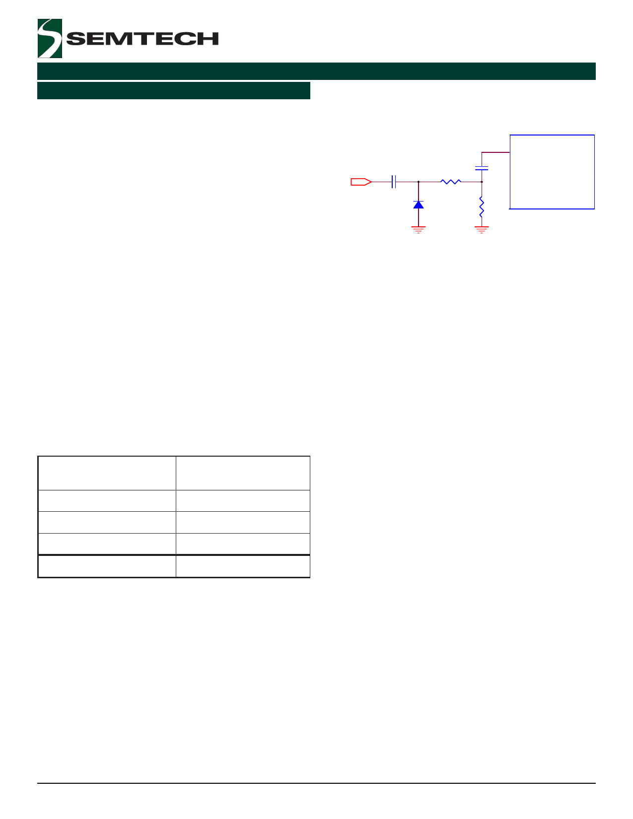
The maximum frequency of the external clock signal can
be higher than the natural switching frequency by about
10%.
External
Clock
Signal
C
56pF
CFSET
R
1k
A
D
RSYNC
100
FSET
SC4608
Oscillator
Figure 1
The FSET pin is used to set the PWM oscillator frequency
through an external timing capacitor that is connected
from the FSET pin to the GND pin. The resulting ramp
waveform ion the FSET pin is a triangle at the PWM fre-
quency with a peak voltage of 1.3V and a valley voltage
of 0.3V. 160ns minimum OFF time for the top switch
allows the bootstrap capacitor to be charged during each
cycle. The capacitor tolerance adds to the accuracy of
the oscillator frequency. The approximate operating fre-
quency and soft start time are both determined by the
value of the external timing capacitor as shown in Table
1.
UVLO
When the EN pin is not pulled and held below 0.3*AVDD,
the voltage on the AVDD pin determines the operation of
the SC4608. As AVDD increases during start up, the UVLO
block senses AVDD and keeps the high side and low side
MOSFETs off and the internal soft start voltage low until
AVDD reaches 2.7V. If no faults are present, the SC4608
will initiate a soft start when AVDD exceeds 2.7V. A hyster-
esis (350mV) in the UVLO comparator provides noise im-
munity during its start up.
External Timing
Capacitor Value (pF)
120
270
470
560
Frequency (kHz)
1000
575
350
295
Table 1. Operating Frequency value Based on the
Value of the External Timing Capacitor Placed Across
the FSET and GND Pins
Synchronous mode operation is invoked by using a sig-
nal from an external clock. A low value resistor (100Ω
typical) must be inserted in series with the timing capaci-
tor between the timing capacitor and the GND pin. The
other terminal of the timing capacitor will remain con-
nected to the FSET pin. The transformed external clock
signal is then connected to the junction of the external
timing capacitor and the added resistor RSYNC as shown
in Figure 1.
Power Good Indicator
The PGOOD pin is the open-drain output of the power
good comparators. These comparators are incorporated
with small amount of hysteresis. A pull-up resistor from
the PGOOD pin to the input supply or the output sets the
logic high level of the PGOOD signal. The VSENSE low-to-
high trip voltage of the power good comparator is 89%
of the final regulation voltage. The power good compara-
tor output becomes valid provided that VO is within about
±11% of the programmed output voltage. In shutdown
mode the power good output is actively pulled low. The
PGOOD signal delay depends on its operating frequency
fs, for example, about 14ms@ fs=575kHz and 24ms @
fs=330kHz.
Soft Start
The soft start function is required for step down control-
lers to prevent excess inrush current through the DC bus
during start up. Generally this can be done by sourcing a
controlled current into a timing capacitor and then using
the voltage across this capacitor to slowly ramp up the
error amp reference. The closed loop creates narrow
2006 Semtech Corp.
8
www.semtech.com
Share Link: 