PDI1394L21BE データシートの表示(PDF) - Philips Electronics
部品番号
コンポーネント説明
一致するリスト
PDI1394L21BE Datasheet PDF : 52 Pages
| |||
Philips Semiconductors
1394 full duplex AV link layer controller
Preliminary specification
PDI1394L21
9.4.1 Bushold and Link/PHY single capacitor
galvanic isolation
9.4.1.1 Bushold
The PDI1394L21 uses an internal bushold circuit on each of the
indicated pins to keep these CMOS inputs from “floating” while being
driven by a 3-Stated device or input coupling capacitor.
Unterminated high impedance inputs react to ambient electrical
noise which cause internal oscillation and excess power supply
current draw.
The following pins have bushold circuitry enabled when the ISO_N
pin is in the logic “1” state:
Pin No.
47
46
54
43
42
41
40
37
36
35
34
Name
PHYCTL0
PHYCTL1
LREQ
PHYD0
PHYD1
PHYD2
PHYD3
PHYD4
PHYD5
PHYD6
PHYD7
Function
PHY control line 0
PHY control line 1
Link request line
PHY data bus bit 0
PHY data bus bit 1
PHY data bus bit 2
PHY data bus bit 3
PHY data bus bit 4
PHY data bus bit 5
PHY data bus bit 6
PHY data bus bit 7
Philips bushold circuitry is designed to provide a high resistance
pull-up or pull-down on the input pin. This high resistance is easily
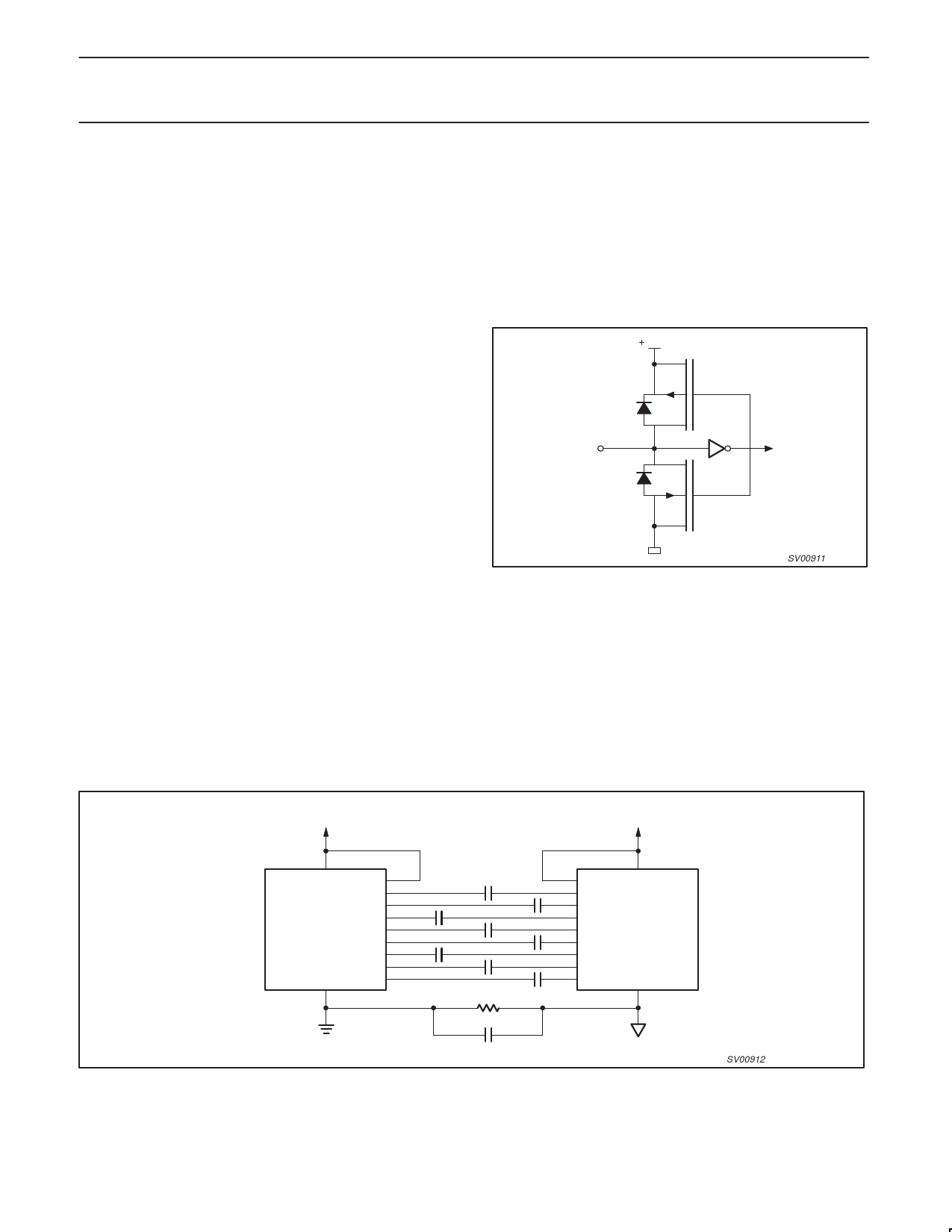
overcome by the driving device when its state is switched. Figure 1
shows a typical bushold circuit applied to a CMOS input stage. Two
weak MOS transistors are connected to the input. An inverter is also
connected to the input pin and supplies gate drive to both
transistors. When the input is LOW, the inverter output drives the
lower MOS transistor and turns it on. This re-enforces the LOW on
the input pin. If the logic device which normally drives the input pin
were to be 3-Stated, the input pin would remain “pulled-down” by the
weak MOS transistor. If the driving logic device drives the input pin
HIGH, the inverter will turn the upper MOS transistor on,
re-enforcing the HIGH on the input pin. If the driving logic device is
then 3-Stated, the upper MOS transistor will weakly hold the input
pin HIGH.
The PHY’s outputs can be 3-Stated and single capacitor isolation
can be used with the Link; both situations will allow the Link inputs to
float. With bushold circuitry enabled, these pins are provided with dc
paths to ground, and power by means of the bushold transistors;
this arrangement keeps the inputs in known logical states.
INPUT PIN
INTERNAL
CIRCUITS
Figure 1. Bushold circuit
SV00911
9.4.1.2 Single capacitor isolation
The circuit example (Figure 2) shows the connections required to
implement basic single capacitor Link/PHY isolation.
NOTE: The isolation enablement pins on both devices are in their
“1” states, activating the bushold circuits on each part. The bushold
circuits provide local dc ground references to each side of the
isolating/coupling capacitors. Also note that ground
isolation/signal-coupling must be provided in the form of a parallel
combination of resistance and capacitance as indicated in
IEEE 1394–1995.
APPLICATION
+3.3V
ISOLATED
+3.3V
6, 13, 24, 32, etc.
ISO_N
PHY D0
48
43
LINK
PHY D1 42
PDI1394L21
PHY D2
PHY D3
41
40
PHYCTL0
PHYCTL1
47
46
LREQ 54
SCLK 55
APPLICATION GROUND
Cc
Cc
Cc
Cc
Cc
1MEG Ω
Cr
ISO–
D0
Cc
D1
PHY
D2 PDI1394Pxx
D3
Cc
PHYCTL0
PHYCTL1
LREQ
Cc
SYSCLK
ISOLATED PHY GROUND
Cc = 0.001µF; Cr = 0.1µF
Figure 2. Single capacitor Link/PHY isolation
SV00912
1999 Aug 06
7
Share Link: 