PDI1394L21 データシートの表示(PDF) - Philips Electronics
部品番号
コンポーネント説明
一致するリスト
PDI1394L21 Datasheet PDF : 52 Pages
| |||
Philips Semiconductors
1394 full duplex AV link layer controller
Preliminary specification
PDI1394L21
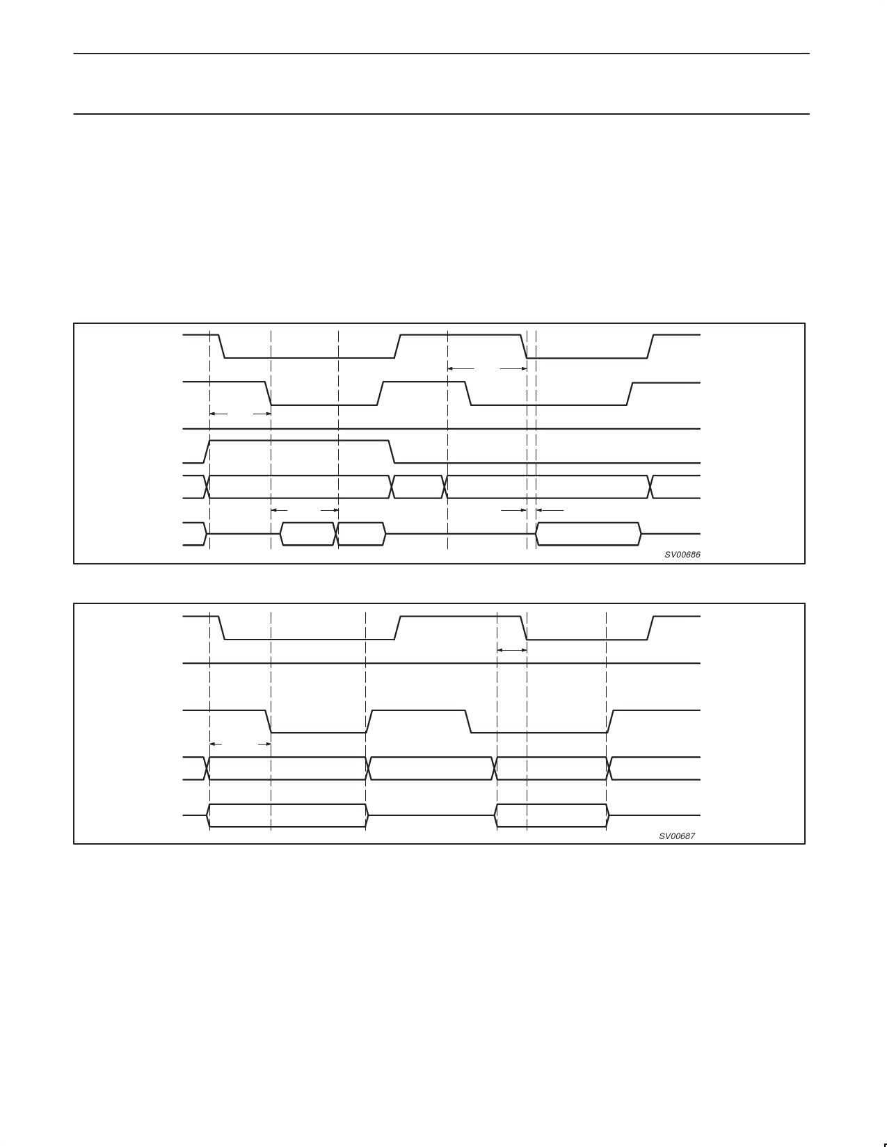
12.3.5 The CPU bus interface signals
The CPU interface is directly compatible with an 8051 microcontroller. It uses a separate HIF RD_N and HIF WR_N inputs and a HIF CS_N chip
select line, all of which are active LOW. There are 9 address inputs (HIF A0..HIF A8) and 8 data in/out lines HIF D0..HIF D7. An open drain
HIF INT_N output is used to signal interrupts to the CPU.
The CPU is not required to run at a clock that is synchronous to the 1394 base clock. The control signals will be resampled by the host interface
before being used internally.
An access through the host interface starts when HIF CS_N = 0 and either HIF WR_N = 0 or HIF RD_N = 0. Typically the chip select signal is
derived from the upper address lines of the CPU (address decode stage), but it could also be connected to a port pin of the CPU to avoid the
need for an external address decoder in very simple CPU systems. When both HIF CS_N = 0 and HIF RD_N = 0 the host interface will start a
read access cycle, so the cycle is triggered at the falling edge of either HIF CS_N or HIF RD_N, whichever is later.
HIF CS_N
HIF RD_N
HIF WR_N
HIF A8
HIF A0..HIF A7
HIF D0..HIF D7
TAS
TAS
TACC
RSRO
RSRn
TACC
RSRn
Figure 4. Read cycle signal timing (2 independent read cycles)
SV00686
HIF CS_N
HIF RD_N
TAS
HIF WR_N
HIF A0..HIF A8
TAS
<VALID ADDRESS>
<VALID ADDRESS>
HIF D0..HIF D7
<WRITE DATA>
<WRITE DATA>
Figure 5. Write cycle signal timing (2 independent write cycles)
SV00687
12.4 The Asynchronous Packet Interface
The PDI1394L21 provides an interface to asynchronous data packets through the registers in the host interface. The format of the
asynchronous packets is specified in the following sections.
12.4.1 Reading an Asynchronous Packet
Upon reception of a packet, the packet data is stored in the appropriate receive FIFO, either the Request or Response FIFO. The location of the
packet is indicated by either the RREQQQAV or RRSPQAV status bit being set in the Asynchronous Interrupt Acknowledge (ASYINTACK)
register. The packet is transferred out of the FIFO by successive reads of the Asynchronous Receive Request (RREQ) or Asynchronous
Receive Response (RRSP) register. The end of the packet (the last quadlet) is indicated by either the RREQQLASTQ or RRSPQLASTQ bit set
in ASYINTACK. Attempting to read the FIFO when either RREQQQAV bit or RRSPQQAV bit is set to 0 (in the Asynchronous RX/TX interrupt
acknowledge (ASYINTACK) register) will result in a queue read error.
1999 Aug 06
12
Share Link: 