PDI1394L21 データシートの表示(PDF) - Philips Electronics
部品番号
コンポーネント説明
一致するリスト
PDI1394L21 Datasheet PDF : 52 Pages
| |||
Philips Semiconductors
1394 full duplex AV link layer controller
Preliminary specification
PDI1394L21
12.3 The host interface
The host interface allows an 8 bit CPU to access all registers and the asynchronous packet queues. It is specifically designed for an 8051
microcontroller but can also be used with other CPUs. There are 64 register addresses (for quadlet wide registers). To access bytes rather than
quadlets the address spaces is 256 bytes, requiring 8 address lines.
The use of an 8 bit interface introduces an inherent problem that must be solved: register fields can be more than 8 bits wide and be used
(control) or changed (status) at every internal clock tick. If such a field is accessed through an 8 bit interface it requires more than one read or
write cycle, and the value should not change in between to maintain consistency. To overcome this problem accesses to the chip’s internal
register space are always 32 bits, and the host interface must act as a converter between the internal 32 bit accesses and external 8 bit
accesses. This is where the shadow registers are used.
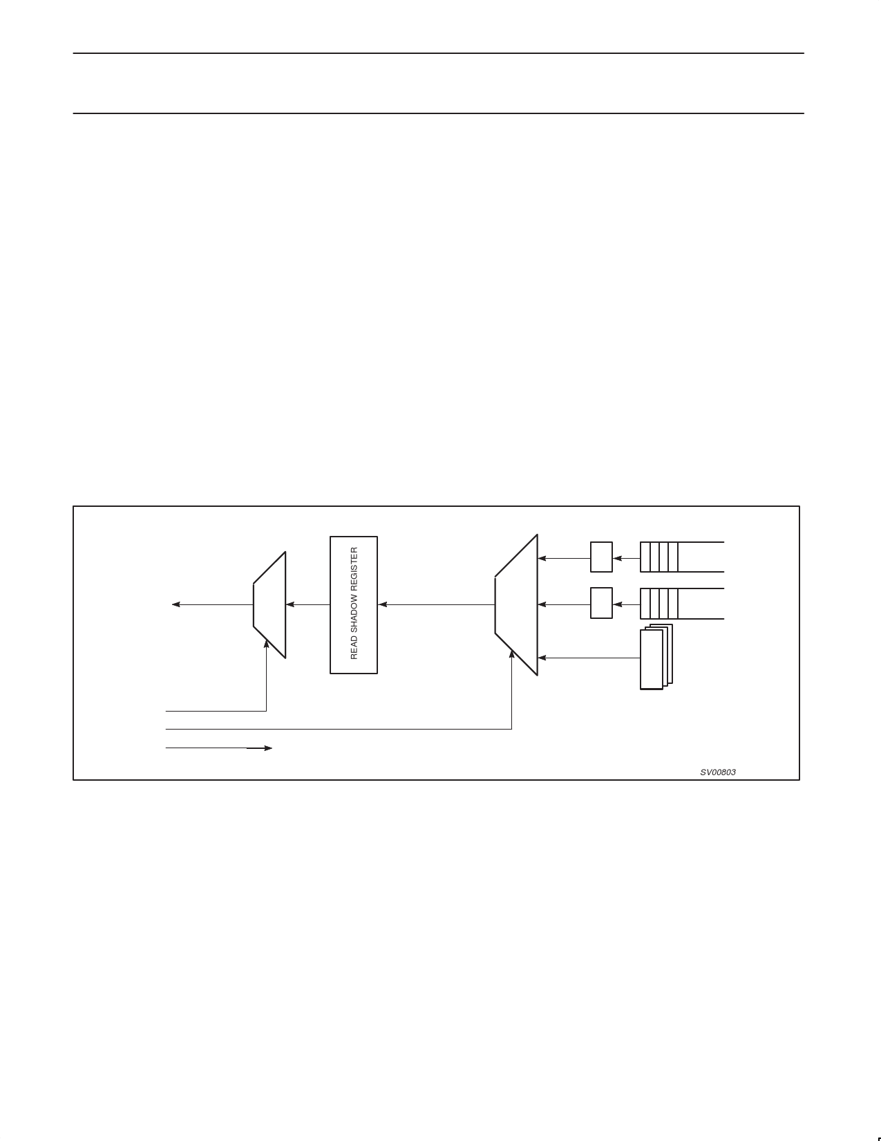
12.3.1 Read accesses
To read an internal register the host interface can make a snapshot (copy) of that specific register which is then made available to the CPU 8
bits at a time. The register that holds the snapshot copy of the real register value inside the host interface is called the read shadow register.
During a read cycle address lines HIF A0 and HIF A1 are used to select which of the 4 bytes currently stored in the read shadow register is
output onto the CPU data bus. This selection is done by combinatorial logic only, enabling external hardware to toggle these lines through
values 0 to 3 while keeping the chip in a read access mode to get all 4 bytes out very fast (in a single extended read cycle), for example into an
external quadlet register.
This solution requires a control line to direct the host interface to make a snapshot of an internal register when needed, as well as the internal
address of the target register. The register address is connected to input address lines HIF A2..HIF A7, and the update control line to input
address line HIF A8. To let the host interface take a new snapshot the target address must be presented on HIF A2..HIF A7 and HIF A8 must be
raised while executing a read access. The new value will be stored in the read shadow register and the selected byte (HIF A0, HIF A1)
appears on the output.
MUX
8
32
CPU
TR
MUX
Q
32
Q
REGISTERS
32
HIF A0..1
HIF A2..7
HIF A8
UPDATE/COPY CONTROL
SV00803
NOTES:
1. It is not required to read all 4 bytes of a register before reading another register. For example, if only byte 2 of register 0x54 is required a
read of byte address 0x100 + (0×54) + 2 = 0x156 is sufficient.
2. The update control line does not necessarily have to be connected to the CPU address line HIF A8. This input could also be controlled by
other means, for example a combinatorial circuit that activates the update control line whenever a read access is done for byte 0. This
makes the internal updating automatic for quadlet reading.
3. Reading the bytes of the read shadow register can be done in any order and as often as needed.
1999 Aug 06
10
Share Link: 