PCF2105 データシートの表示(PDF) - Philips Electronics
部品番号
コンポーネント説明
一致するリスト
PCF2105 Datasheet PDF : 48 Pages
| |||
Philips Semiconductors
LCD controller/driver
Product specification
PCF2105
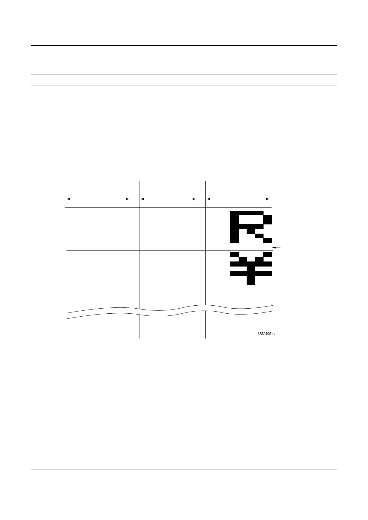
handbook, full pagewidth
character codes
(DDRAM data)
76 5 43 2 10
higher
order
bits
lower
order
bits
00 0 00 0 00
00 0 00 0 01
00 0 00 0 10
CGRAM
address
6 5 43 2 10
higher
order
bits
lower
order
bits
00 0 00 0 0
001
010
011
100
101
110
111
00 0 10 0 0
001
010
011
100
101
110
111
0 0 1 00 0 0
001
00 0 01 1 11
00 0 01 1 11
00 0 01 1 11
00 0 01 1 11
1111100
1111101
1111110
1111111
character patterns
(CGRAM data)
higher
order
bits
4 3 21 0
lower
order
bits
0
0 00
0 00
0
0
00
00
0
0 00
0 0 00 0
0 00
0
0
0
00
00
00
00
00
00
0 0 00 0
character
pattern
example 1
cursor
position
character
pattern
example 2
MGA800 - 1
Character code bits 0 to 3 correspond to CGRAM address bits 3 to 6.
CGRAM address bits 0 to 2 designate character pattern line position. The 8th line is the cursor position and display is performed by logical OR with the
cursor. Data in the 8th line will appear in the cursor position.
Character pattern column positions correspond to CGRAM data bits 0 to 4; bit 4 being at the left end, as shown in this figure.
CGRAM character patterns are selected when character code bits 4 to 7 are all logic 0. CGRAM data is logic 1 corresponds to selection for display.
Only bits 0 to 5 of the CGRAM address are set by the ‘set CGRAM address’ instruction. Bit 6 can be set using the ‘set DDRAM address’ instruction or
by using the auto-increment feature during CGRAM write. All bits 0 to 6 can be read using the ‘read busy flag and address’ instruction.
Fig.6 Relationship between CGRAM addresses, data and display patterns.
1998 Jul 30
11
Share Link: 