P4C164L-100CMB データシートの表示(PDF) - Semiconductor Corporation
部品番号
コンポーネント説明
一致するリスト
P4C164L-100CMB Datasheet PDF : 16 Pages
| |||
AC TEST CONDITIONS
Input Pulse Levels
Input Rise and Fall Times
Input Timing Reference Level
Output Timing Reference Level
Output Load
GND to 3.0V
3ns
1.5V
1.5V
See Figures 1 and 2
P4C164
TRUTH TABLE
Mode
CE
1
CE2
OE
Standby H X X
Standby X L X
DOUT
Disabled L
HH
Read
L HL
Write
L HX
WE I/O Power
X High Z Standby
X High Z Standby
H High Z Active
H DOUT Active
L High Z Active
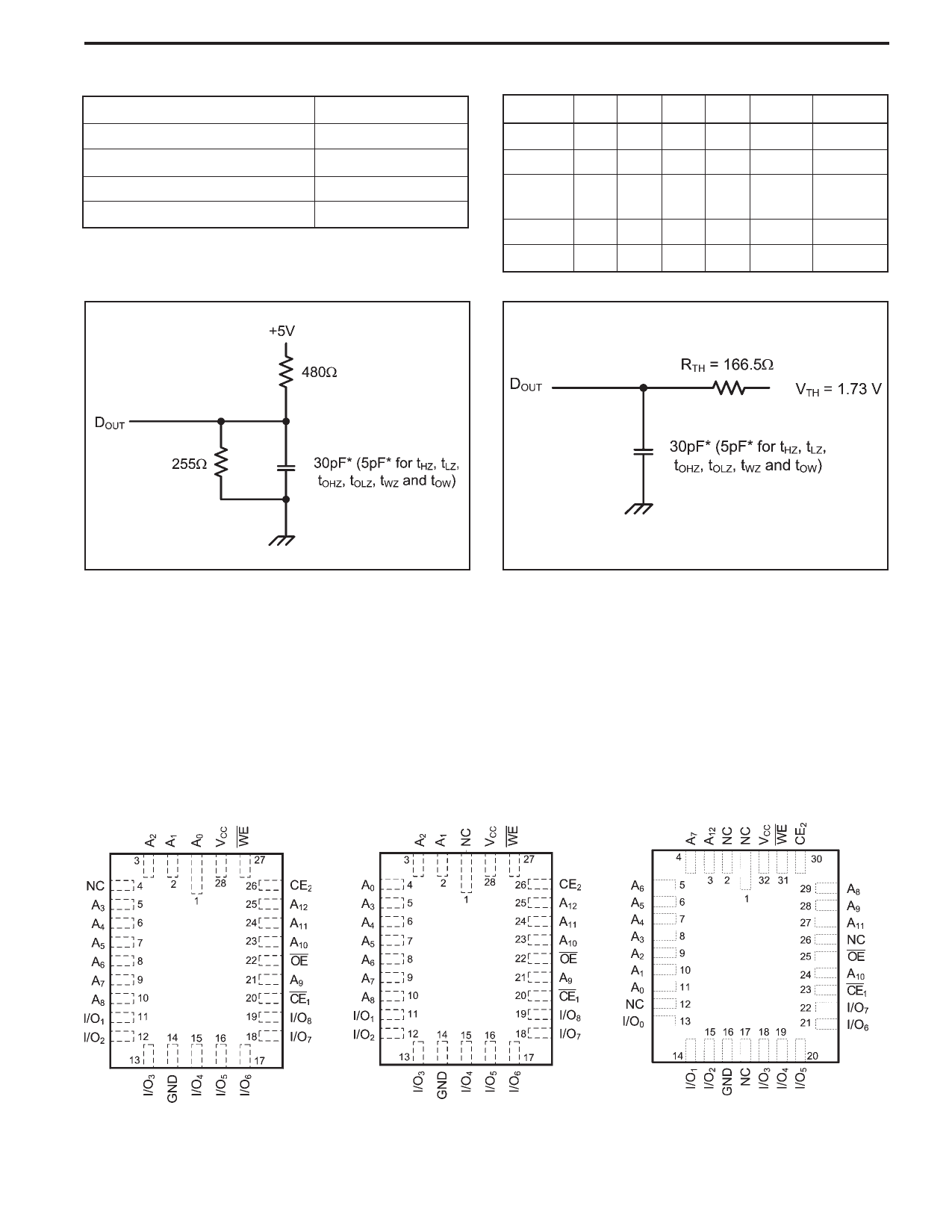
Figure 1. Output Load
* including scope and test fixture.
Note:
Because of the high speed of the P4C164/L, care must be taken when
testing this device; an inadequate setup can cause a normal functioning
part to be rejected as faulty. Long high-inductance leads that cause
supply bounce must be avoided by bringing the VCC and ground planes
directly up to the contactor fingers. A 0.01 µF high frequency capacitor
is also required between VCC and ground. To avoid signal reflections,
Figure 2. Thevenin Equivalent
proper termination must be used; for example, a 50Ω test environment
should be terminated into a 50Ω load with 1.73V (Thevenin Voltage) at
the comparator input, and a 116Ω resistor must be used in series with
DOUT to match 166Ω (Thevenin Resistance).
LCC PIN CONFIGURATIONS
LCC (L5)
"L" - STANDARD PIN-OUT
Document # SRAM115 REV F
LCC (L5)
"LS" - SPECIAL PIN-OUT
LCC (L6)
Page 7 of 16
Share Link: 