NJU3505L データシートの表示(PDF) - Japan Radio Corporation
部品番号
コンポーネント説明
一致するリスト
NJU3505L Datasheet PDF : 64 Pages
| |||
NJU3505
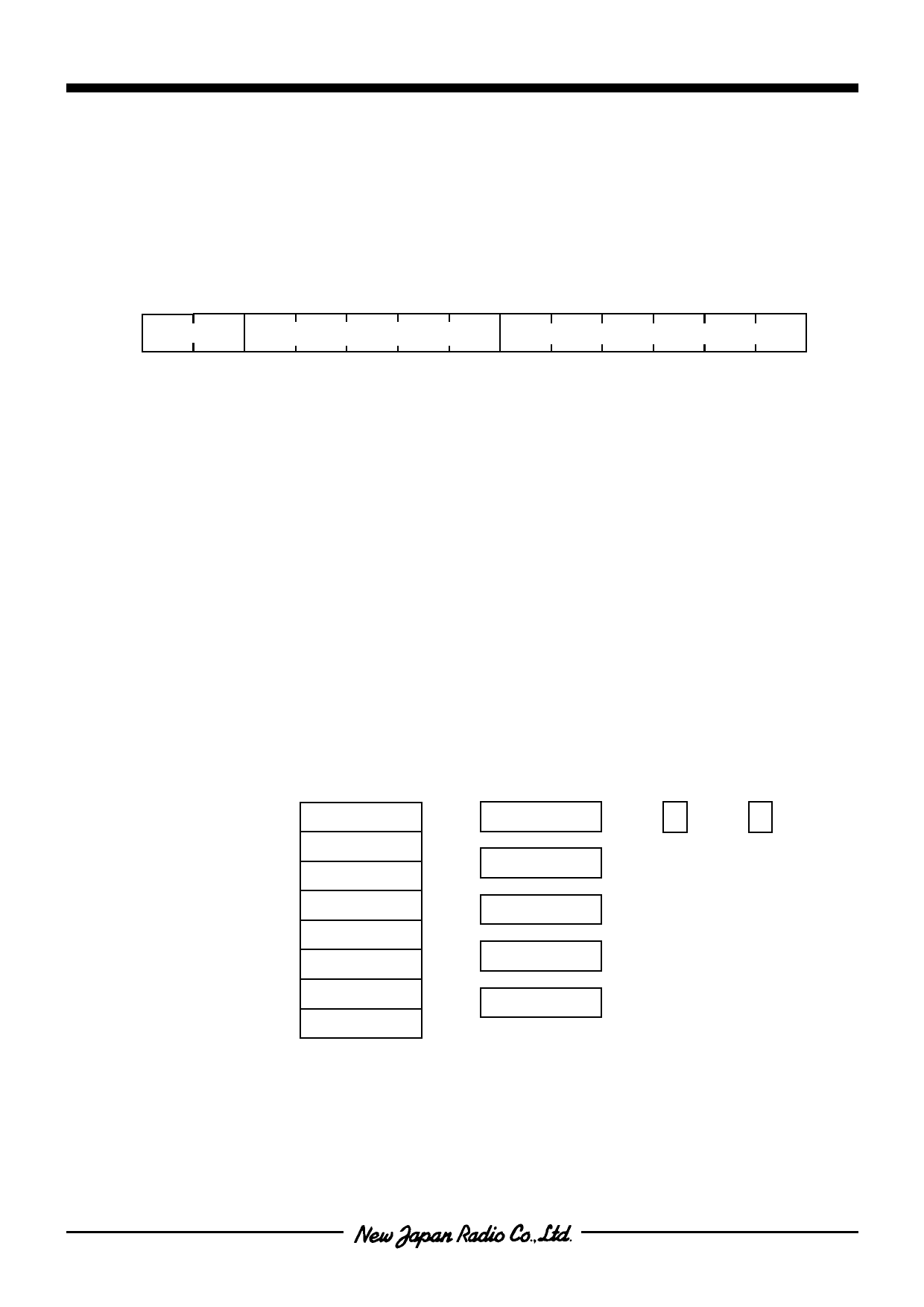
s PROGRAM COUNTER(PC)
PROGRAM COUNTER(PC) consisted of the 13-bit binary counter stores the address for the next
operating instruction in ROM. Data figures limited from b0 to b5 on the PC indicate the address in a page,
and data figures limited from b6 to b10 on the PC indicate the page in a bank, and data figures limited
from b11 to b12 on PC indicates a bank in ROM. Although the ROM address can be indicated 8192
addresses continuously, the target address of JMP instruction is restricted by Paging structure in ROM.
The target address of JPL or CALL instruction is restricted by Banking structure in ROM.
The PC condition is set to “0” on the “RESET” operation.
(MSB) 12 11 10
9
8
7
6
5
4
3
2
1
0 (LSB)
Bank allocation
Page allocation
Address location
JMP instruction can branch to the optional address in the page. The target address is indicated by the
data figures limited from b0 to b5(6 bits) on PC as shown in above. The paging structure can reduce the
program size in ROM and the JMP instruction execution time against JPL instruction because JMP
instruction is consisted of one byte(8 bits) length. JPL and CALL instructions can branch to the optional
address without considering the paging structure, because they consist of two bytes(16 bits) length
including the 11 bits of PC. But JPL and CALL instructions can not branch between the banks in ROM.
The memory bank register(PHY15) on the peripheral register table0 selects a bank in ROM. When the
branch target address is not found in the bank, the memory bank register requires to change the bank
number.
• STACK
STACK consists of three types of registers which are the 8 by 13 bits, the 5 by 4 bits, and the 2 by 1 bit
registers. The registers of STACK hold the data of PC automatically when the interrupt routine or the
subroutine is called. The 5 by 4 bits registers of STACK hold the data of the internal registers
automatically when the interrupt operation is executed. The 2 by 1 bit registers of STACK hold the data of
the internal flag automatically when the interrupt operation is executed. In the return (RET or RETI)
operation, PC, the internal registers, and the internal flags registers get the held data from STACK
automatically.
[ For branch(CALL) and interrupt operation ] [ For interrupt operation ]
STACK POINTER 12
0
000
PC
001
PC
010
PC
011
PC
100
PC
101
PC
110
PC
111
PC
3
0
AC
X-register
X'-register
Y-register
Y'-register
0
0
RPC
STATUS
-9-
Share Link: 