NJU3505L データシートの表示(PDF) - Japan Radio Corporation
部品番号
コンポーネント説明
一致するリスト
NJU3505L Datasheet PDF : 64 Pages
| |||
NJU3505
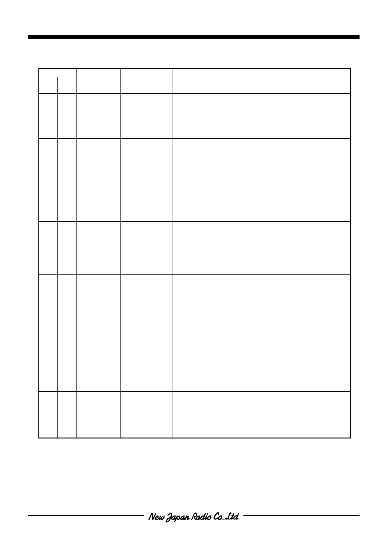
s TERMINAL DESCRIPTION 3
No.
NJU NJU
SYMBOL INPUT/OUTPUT
FUNCTION
3505F 3505L
24 27
SCK /
CKOUT
SCK :INOUT Selects a function of either of 1) or 2) by the mask option.
CKOUT :
1) Serial Clock Input or Output Terminal with Pull-up
OUTPUT Resistance. (SCP, SC)
2) Clock Divided by Prescaler Output Terminal.
Selects the dividing times of the clock in the prescaler by
the mask option.
25 28
26 29
27 30
28 31
AIN4/PA0
AIN5/PA1
AIN6/PA2
AIN7/PA3
PA0: INOUT
AIN4: INPUT
PA1: INOUT
AIN5: INPUT
PA2: INOUT
AIN6: INPUT
PA3: INOUT
AIN7: INPUT
4-bit Programmable Input / Output PORTA.
Selects a function of either of 1) or 2) for PORTA by the
mask option.
1) 4-bit Analog Input to A/D Converter. (AD)
2) 4-bit Input / Output Terminals as PORTA.
These 4-bit terminals direction can be changed by the
program as 4-Input or 4-Output.
Use of Pull-up resistance for a terminal is in accordance
with the mask option.
•as Input : C-MOS Input Terminals (IOP)
•as Output: Nch-FET Open-Drain Output Terminals (IO)
29 32
PB0
30 33
PB1
31 34
PB2
32 35
PB3
INOUT
4-bit Programmable Input / Output PORTB.
These 4-bit terminals direction can be changed by the
program as 4-Input or 4-Output.
Use of Pull-up resistance for a terminal is in accordance
with the mask option.
•as Input : C-MOS Input Terminals (IOP)
•as Output: Nch-FET Open-Drain Output Terminals (IO)
33 36
34 37
35 38
VDD
–
Power Source (2.4V − 5.5V)
PC0
INPUT/OUTPUT 2-bit Input / Output PORTC.
PC1
Selects a terminal circuit for each port from the following
by the mask option.
•C-MOS Input Terminal with Pull-up Resistance (ICP)
•C-MOS Input Terminal (IC)
•Nch-FET Open-Drain Output Terminal with Pull-up
Resistance (ONP)
•Nch-FET Open-Drain Output Terminal (ON)
36 39
37 40
38 41
39 42
PD0
INPUT/OUTPUT 4-bit Input / Output PORTD.
PD1
Selects a terminal circuit for each port from the following
PD2
by the mask option.
PD3
•C-MOS Input Terminal with Pull-up Resistance (ICP)
•C-MOS Input Terminal (IC)
•C-MOS Output Terminal (OC)
40 1
41 2
42 3
43 4
PE0
INPUT/OUTPUT 4-bit Input / Output PORTE.
PE1
Selects a terminal circuit for each port from the following
PE2
by the mask option.
PE3
•C-MOS Input Terminal with Pull-up Resistance (ICP)
•C-MOS Input Terminal (IC)
•C-MOS Output Terminal (OC)
Note )INPUT/OUTPUT : Input or Output is selected by the mask option.
INOUT : Input or Output is changed by the program.
“AD, IC, ICP, II, IIP, IO, IOP, IS, ISP, OC, ON, ONP, SC, SCP, SD, SDP, SO” are symbols using on MASK
OPTION GENERATOR(MOG).
-6-
Share Link: 